Differential amplifier with DC offset cancellation

a technology of offset cancellation and differential amplifier, which is applied in the direction of dc-amplifiers with dc-coupled stages, differential amplifiers, and amplifiers with semiconductor devices/discharge tubes, etc. it can solve the problems of reducing the dc offset and detrimentally saturating the differential output signal vout with invalid information, and achieves low eye-diagram closure, excellent input impedance matching, and good jitter (and bit error rate performance

Inactive Publication Date: 2005-07-05
IBM CORP
View PDF3 Cites 40 Cited by
  • Summary
  • Abstract
  • Description
  • Claims
  • Application Information

AI Technical Summary

Benefits of technology

[0006]In addition to this DC offset signal reduction, the improved amplifier of the present invention offers other outstanding advantages. Because, there the feedback signal does not interfere with the input signal, an excellent input impedance matching is obtained, i.e. the scattering parameter S11 is negative and close to infinite. This is mandatory in high speed systems to achieve a low eye-diagram closure or good jitter (and bit error rate) performance. The efficiency of offset reduction can be adjusted and is independent of input signal amplification. The loop stability is ensured by construction. Finally, all elements can be integrated in a chip using conventional integrated circuit technologies, saving board space, element count and cost.
[0007]It is therefore a primary object of the present invention to provide an improved large bandwidth high frequency differential amplifier having a feedback loop that allows to significantly reduce the DC offset.
[0008]It is another object of the present invention to provide an improved large bandwidth high frequency differential amplifier having a feedback loop wherein the feedback signal does not interfere with the input signal improving thereby the input impedance matching (represented by the S11 parameter).

Problems solved by technology

The conventional differential amplifier shown in FIG. 1 only partially reduces the DC offset, because, unfortunately, it amplifies not only the useful input signal but also any DC offset signal, coming from the previous circuits or internally generated at the input terminals of amplifier 10.
The amplitude of this DC offset signal can be of the same order of magnitude or even greater than the one of the input signal itself and then can detrimentally saturate the differential output signal Vout with invalid information.

Method used


Image

  • Differential amplifier with DC offset cancellation
  • Differential amplifier with DC offset cancellation
  • Differential amplifier with DC offset cancellation

Examples


Embodiment Construction

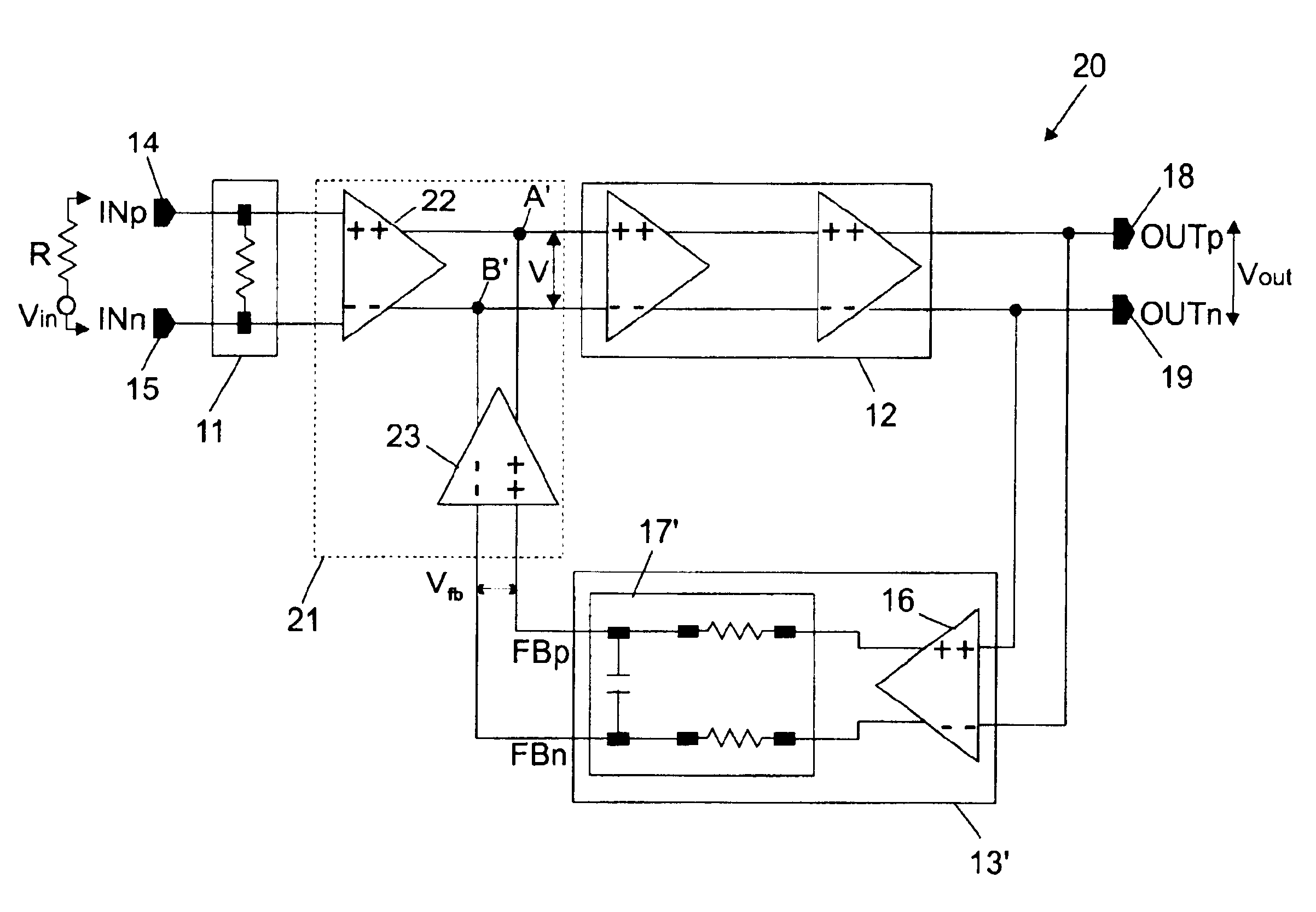
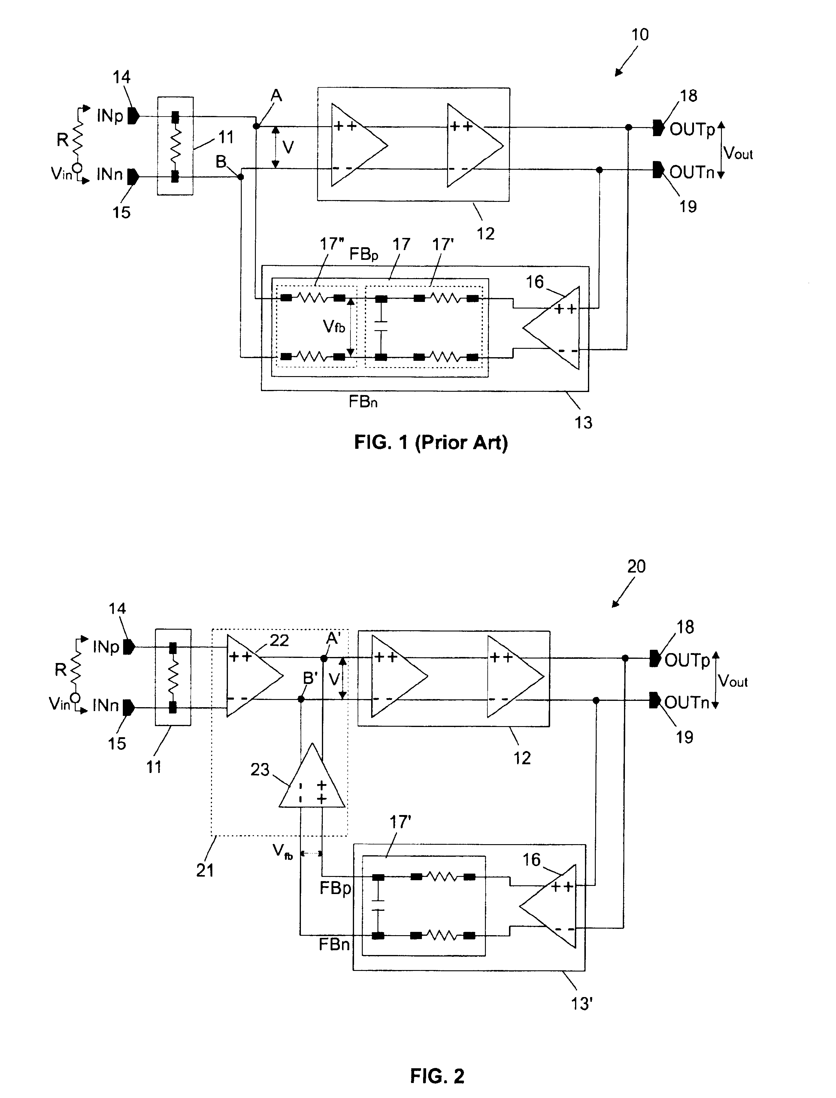
[0014]Like reference numerals (with prime) are used through the several drawings to designate identical (corresponding) parts.

[0015]The improved large bandwidth high frequency amplifier of the present invention is shown in FIG. 2 where its bears numeral 20. In essence, it differs from the conventional FIG. 1 amplifier 10 by the input and feedback signal combining block that bridges both the direct amplification line and the feedback loop, while the other elements remain substantially identical. Now turning to FIG. 2, the signal and feedback signal combining block referenced 21 is comprised of a circuit 22, typically a buffer or an unitary gain amplifier (as shown in the drawing), placed between the input matching circuit 11 and the amplification section 12 on the one hand, and of a differential amplifier 23 connected in series with the feedback block now referenced 13′ because the RC network 17 shown in FIG. 1, can be simplified in some extent (the resistors composing sub-network 17...


PUM


Abstract

There is disclosed an improved differential amplifier (20) having a feedback loop that generates an amplified output signal (Vout) from an input signal (Vin) supplied by a preceding stage. It comprises an input matching circuit (11) connected to said preceding stage, a buffer (22) and an amplification section (12) connected in series in the direct amplification line, a first amplifier (16), a RC network (17′) and a second amplifier (23) connected in series in a parallel loop between the outputs and the inputs of the amplification section that generate the feedback signal. The role of said buffer and second amplifier associated in a dedicated direct and feedback signal combining block (21) is to respectively isolate the input signal and the feedback signal from the summing nodes (A′,B′) at the amplification section inputs. As a result, the summation of the input signal and the feedback signal is improved, the DC component of the output signal is filtered out in order to significantly reduce the DC offset. In addition, the input impedance matching represented by parameter S11 is considerably improved.

Description

BACKGROUND OF INVENTION[0001]The present invention relates to large bandwidth high frequency amplifiers to be placed in the receiver section of a high speed transmission system and more particularly to an improved differential amplifier provided with a parallel feedback loop to amplify high frequency signals wherein the DC offset is significantly reduced and the input impedance matching improved.[0002]In the receiving part of high speed wired transmission systems (like Ethernet), there is a need for the amplification of high frequency low power signals. This is achieved with a dedicated differential amplifier basically consisting of a chain of low gain large bandwidth amplifiers with a parallel feedback loop, usually called post-amplifier or PA, that is placed after the optical circuitry (photodiode and associated transimpedance circuit) of the receiving section.[0003]The block diagram of such a conventional amplifier is shown in FIG. 1. Now turning to FIG. 1, the conventional diffe...

Claims


Application Information

Patent Timeline
Patent Type & Authority Patents(United States)
IPC IPC(8): H03F3/45
CPCH03F3/45278H03F3/45475H03F3/45973H03F2203/45521H03F2203/45652
Inventor GABILLARD, BERTRANDRIVIER, MICHELVOISIN, FABRICEGIRARD, PHILIPPE
Owner IBM CORP
Why Eureka
Try Eureka