Method and apparatus for digital column fixed pattern noise canceling for a CMOS image sensor

a technology of image sensor and fixed pattern, applied in the field of mos image sensor, can solve the problems of decreasing the fixed pattern noise canceling rate of the above circuit, increasing the gain of the signal amplifier, and generating column fixed pattern noise, so as to achieve the effect of free of fixed pattern nois

Inactive Publication Date: 2005-07-05
OMNIVISION TECH INC
View PDF24 Cites 38 Cited by
  • Summary
  • Abstract
  • Description
  • Claims
  • Application Information

AI Technical Summary

Problems solved by technology

Column amplifiers generate column fixed pattern noise due to circuit and process variations.
One problem with the fixed pattern noise compensation method of FIG. 1 is that in low light environments, if the pixel signal is low, then the gain of the signal amplifier must be increased.
If the gain of the signal amplifier is increased, then the fixed pattern noise canceling rate of the above circuit will decrease because of the analog subtraction circuit's inherent errors that result from process variations.

Method used


Image

  • Method and apparatus for digital column fixed pattern noise canceling for a CMOS image sensor
  • Method and apparatus for digital column fixed pattern noise canceling for a CMOS image sensor
  • Method and apparatus for digital column fixed pattern noise canceling for a CMOS image sensor

Examples


Embodiment Construction

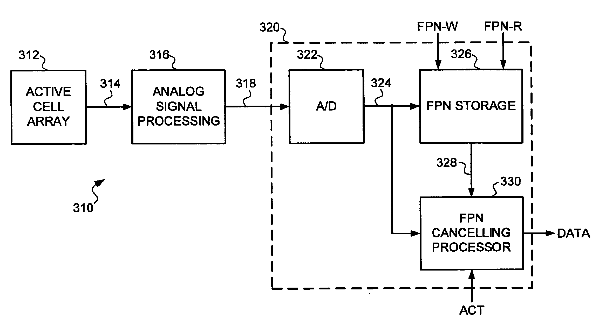
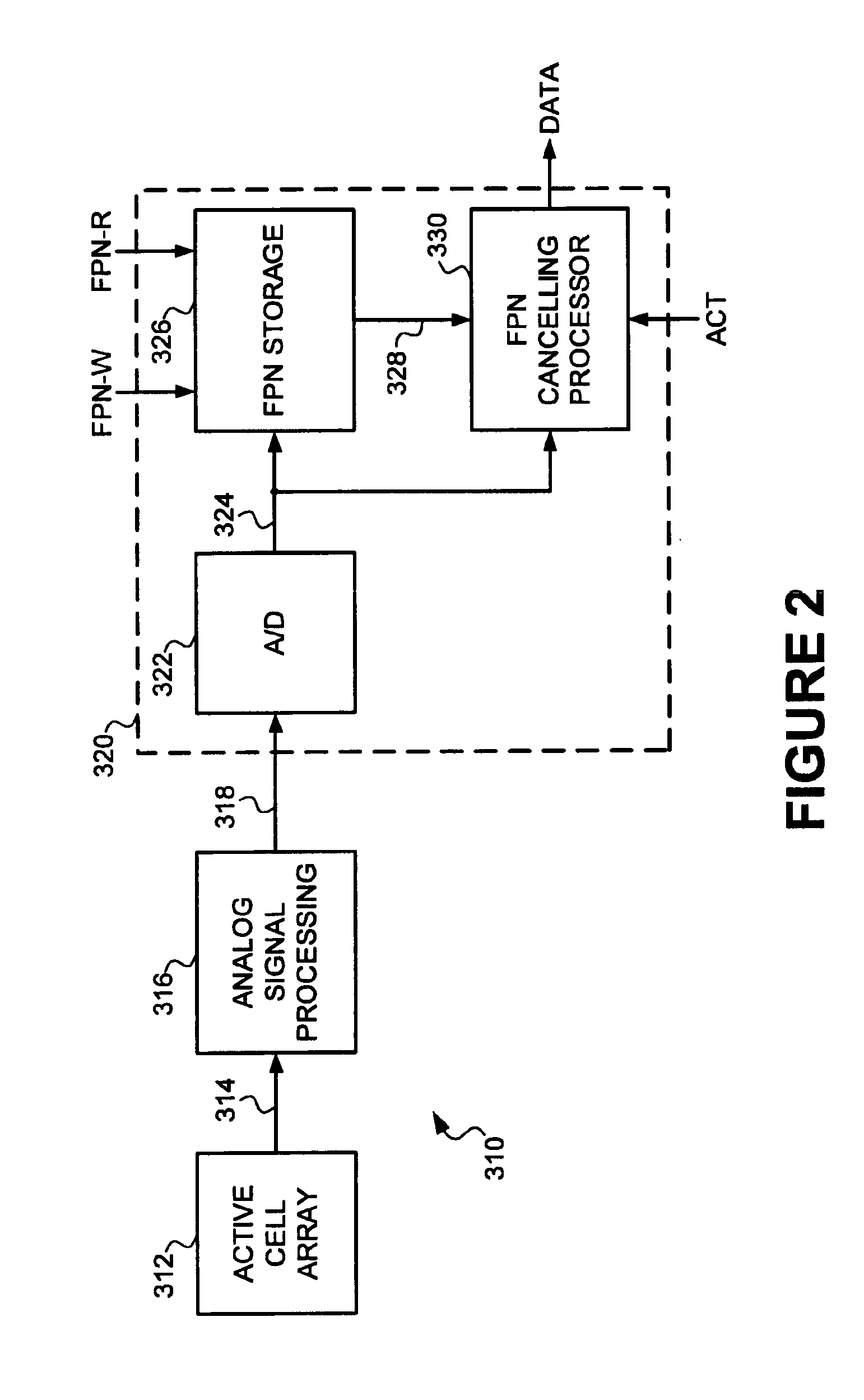
[0019]A CMOS image sensor and readout circuit 310 formed according to the present invention is illustrated in FIG. 2. An active cell array 312 includes a number of pixels organized into rows and columns. The active cell array 312 includes at least one “reference row.” The reference row may be placed at the top or bottom of the active array, or somewhere in between. The reference row is created by using a light shield or black layer to cover the cells of the reference row from light. Thus, the only signal that should be generated from the sensors of the reference row is a noise or dark signal. During the readout process, the exposure time of the reference row is the same as it is for the rest of the rows of the active cell array.

[0020]Signals from the pixels in cell array 312 are read out through a series of reading lines 314 by analog signal processing circuitry 316. A cell array and analog signal processing of the signals are described in more detail in a copending application enti...


PUM


Abstract

The present invention is directed to a method and apparatus for reading out signals from a MOS image sensor. The invention allows for a relatively high fixed pattern noise canceling rate, even in low light environments. The invention includes a digital processing structure for processing the signals from a pixel array. The pixel array includes a reference row that is formed by being covered by a light shield or black layer to cover the pixels of the reference row from light. The signals from the reference row are converted to digital values and stored in fixed pattern noise storage circuitry. Then, as each of the remaining rows of the pixel array are read out, they are converted to digital values and the digital reference row signals are subtracted therefrom to produce data image signals that are relatively free of fixed pattern noise. Thus, the fixed pattern noise canceling rate is made to depend on the precision of an analog-to-digital converter, rather than the process variations of an analog subtraction circuit.

Description

FIELD OF THE INVENTION[0001]The present invention relates to metal oxide semiconductor (MOS) image sensors and, more particularly, to a method and apparatus for reading out image signals from a CMOS image sensor.BACKGROUND OF THE INVENTION[0002]Integrated circuit technology has revolutionized various fields including computers, control systems, telecommunications, and imaging. There are a number of types of semiconductor imagers, including charge coupled devices, photodiode arrays, charge injection devices, and hybrid focal plane arrays. Some sensors are referred to as active pixel image sensors (APS). An active pixel image sensor is defined as an image sensor technology that has one or more active transistors within the pixel unit cell. Some types of active pixel sensor technologies include the amplified MOS imager (AMI), charge modulation device (CMD), volt charge modulated device (VCMD), base stored image sensor (BASIS), and the static induction transistor (SIT).[0003]It is desir...

Claims


Application Information

Patent Timeline
Patent Type & Authority Patents(United States)
IPC IPC(8): H04N9/64H04N5/361H04N5/365H04N5/374H04N5/378
CPCH04N5/365H04N25/67
Inventor DONG, KIMBLE
Owner OMNIVISION TECH INC
Why Eureka
Try Eureka