

Liquid crystal display apparatus of a lateral direction electric field drive type
- Summary
- Abstract
- Description
- Claims
- Application Information
AI Technical Summary
Benefits of technology
Problems solved by technology
Method used
Image

Examples
embodiment 3
[Embodiment 3]
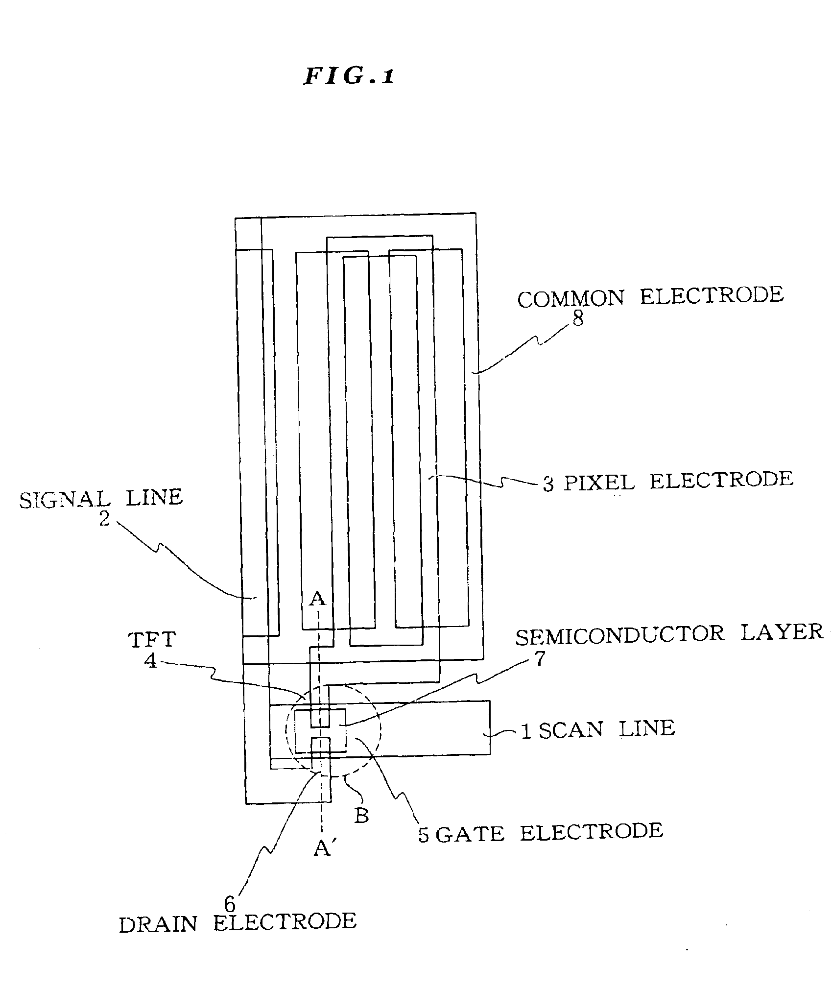
[0095]FIG. 1 is an enlarged plan view of a unit pixel of an active matrix substrate of a liquid crystal display apparatus of the IPS type according to a first embodiment of the present invention. In a region defined by a scan line 1 and a signal line 2 arranged in a matrix shape, a TFT (thin film transistor) 4 and a pixel electrode 3 connected to the TFT are formed. The TFT 4 has a gate electrode 5 on which a semiconductor layer 7 is formed for forming a TFT via an insulation film (not depicted). Furthermore, on these, a pixel electrode (source electrode) 3 and a drain electrode 6 are formed so as to sandwich the semiconductor layer 7. Moreover, the gate electrode 5 is connected to the scan line 1 while the drain electrode 6 is connected to a signal line 2. A reference symbol 8 denotes a common electrode positioned on the same layer as the gate layer.
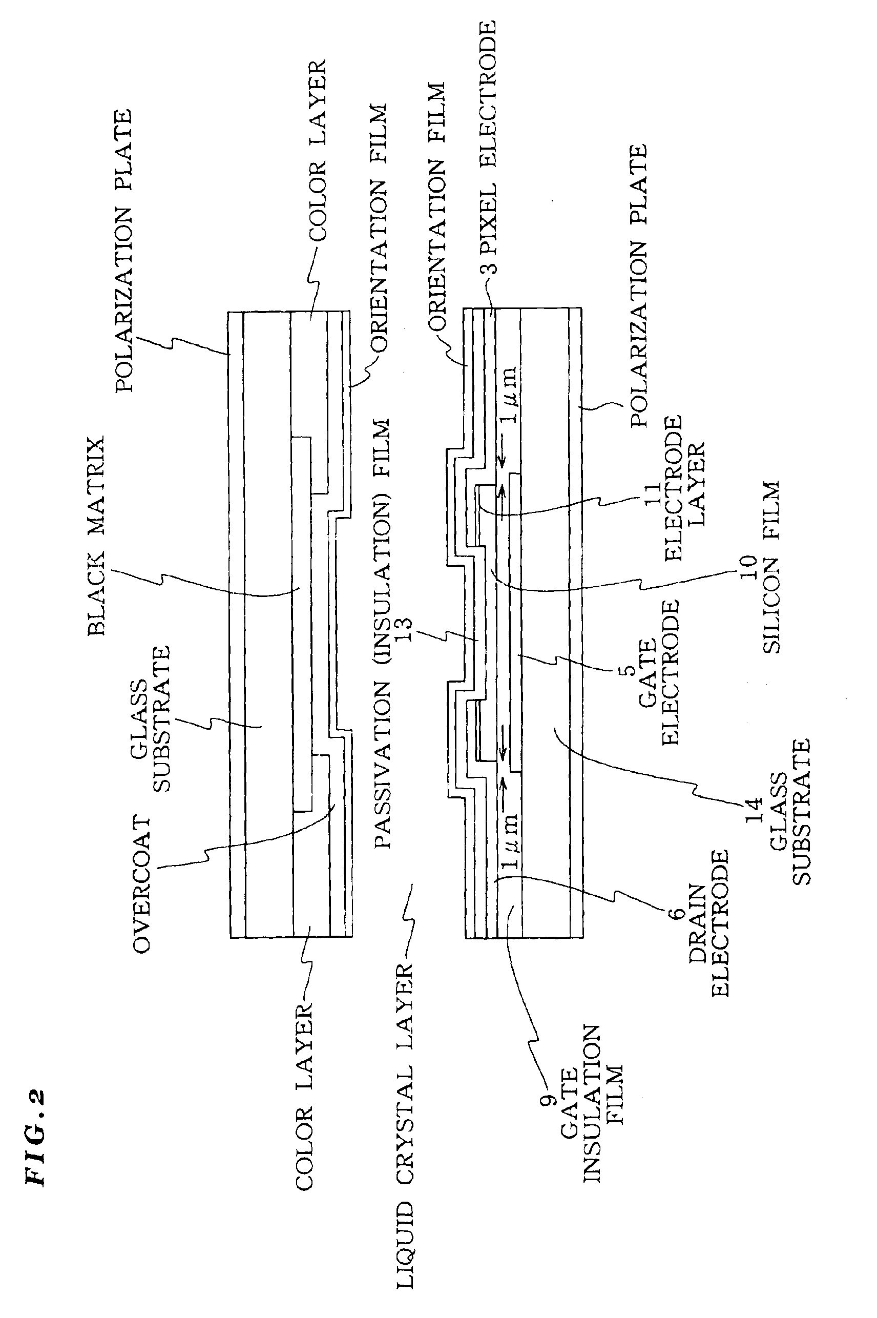
[0096]FIG. 2 is a partial cross sectional view of a liquid crystal display apparatus including an opposing color filter ...
embodiment 4
[Embodiment 4]
[0126]Description will now be directed to a liquid crystal display apparatus according to a forth embodiment of the present invention.
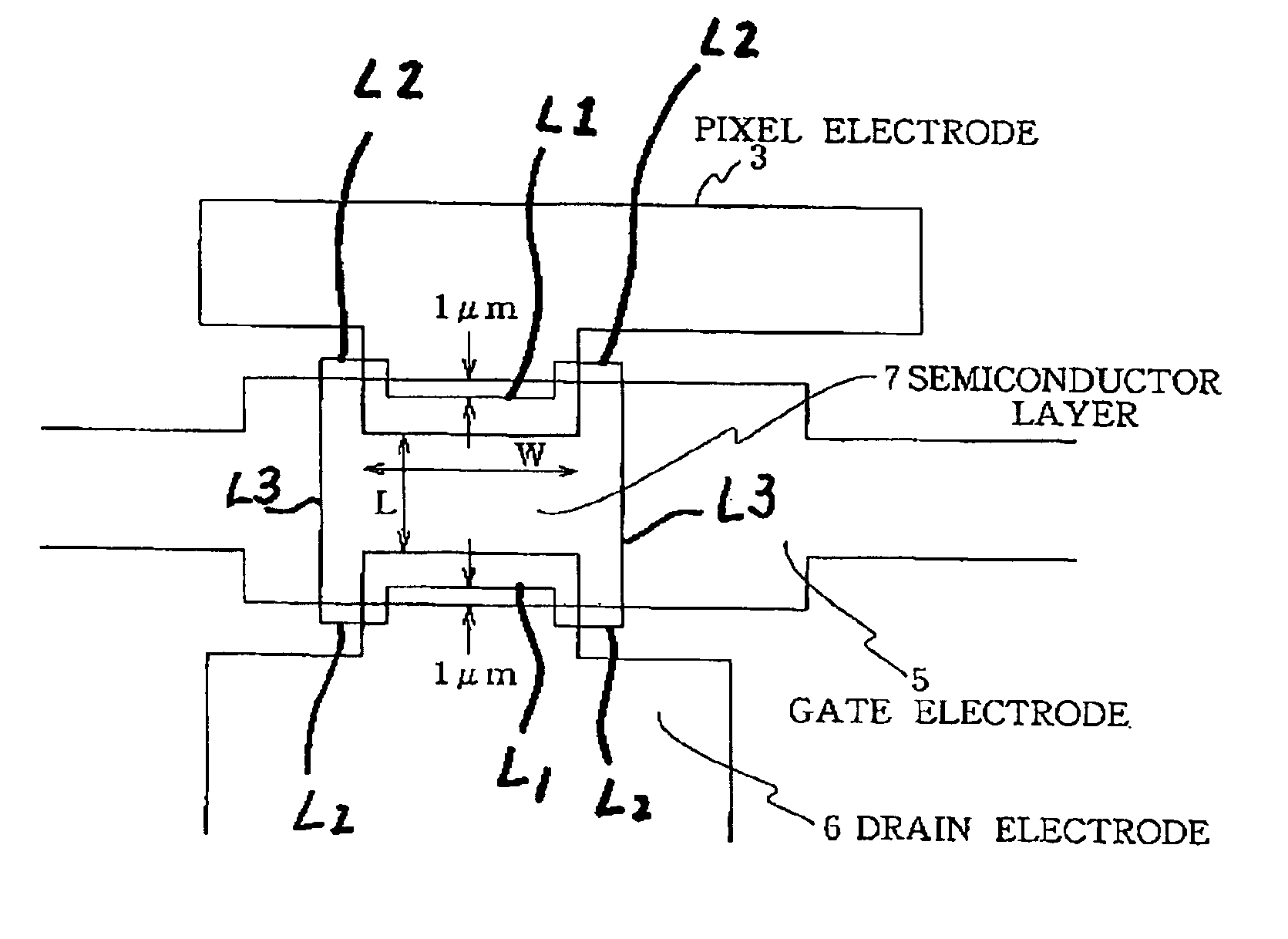
[0127]FIG. 13-20 is an enlarged plan view of a unit pixel of an active matrix substrate of a liquid crystal display apparatus according to the forth embodiment. In a region defined by a scan line 1 and a signal line 2 arranged in a matrix shape, a TFT (thin film transistor) 4 and a pixel electrode connected to the TFT 4 are formed. The TFT 4 has a gate electrode 5 on which a semiconductor is formed for forming the TFT via an insulation film (not depicted). Furthermore, thereon, the semiconductor layer 7 is sandwiched by the pixel electrode (source electrode) 3 and a drain electrode 6 formed in the opposing positions. The gate electrode 5 constitutes a part of the scan line and the drain electrode is connected to the signal line 2.
[0128]FIG. 14-21 is a partial cross sectional view of a liquid crystal display apparatus including an opposin...
PUM
 Abstract
Description
Claims
Application Information