Static semiconductor memory device and method of controlling the same

Active Publication Date: 2005-07-12
SOCIONEXT INC
View PDF7 Cites 4 Cited by
  • Summary
  • Abstract
  • Description
  • Claims
  • Application Information

AI Technical Summary

Benefits of technology

[0025]It is an object of the present invention to provide a static semiconductor memory device which improves the data holding characteristics of a 4Tr SRAM, increases the read speed, decreases write errors, and reduces the standby current, and a method of controlling the same.
[0027]In the static semiconductor memory device and the method of controlling the device according to the present invention, the voltage value representing that the word line connected to the memory cell formed from four transistors is controlled in each of the access mode and non-access mode for the memory cell, thereby adjusting the leakage current between the memory cell and a bit line in each of the access mode and non-access mode. For this reason, the data holding characteristics can be improved, the read speed can be increased, write errors can be suppressed, and the standby current can be reduced.

Problems solved by technology

However, this setting method has the following three problems.
Hence, the read operation cannot be normally executed.
This impedes the speed of read operation increasing.
However, power consumption increases.

Method used


Image

  • Static semiconductor memory device and method of controlling the same
  • Static semiconductor memory device and method of controlling the same
  • Static semiconductor memory device and method of controlling the same

Examples


first embodiment

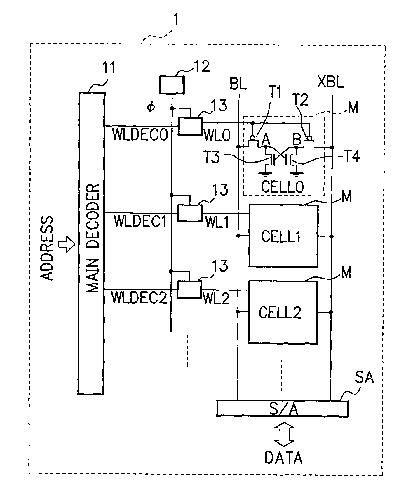
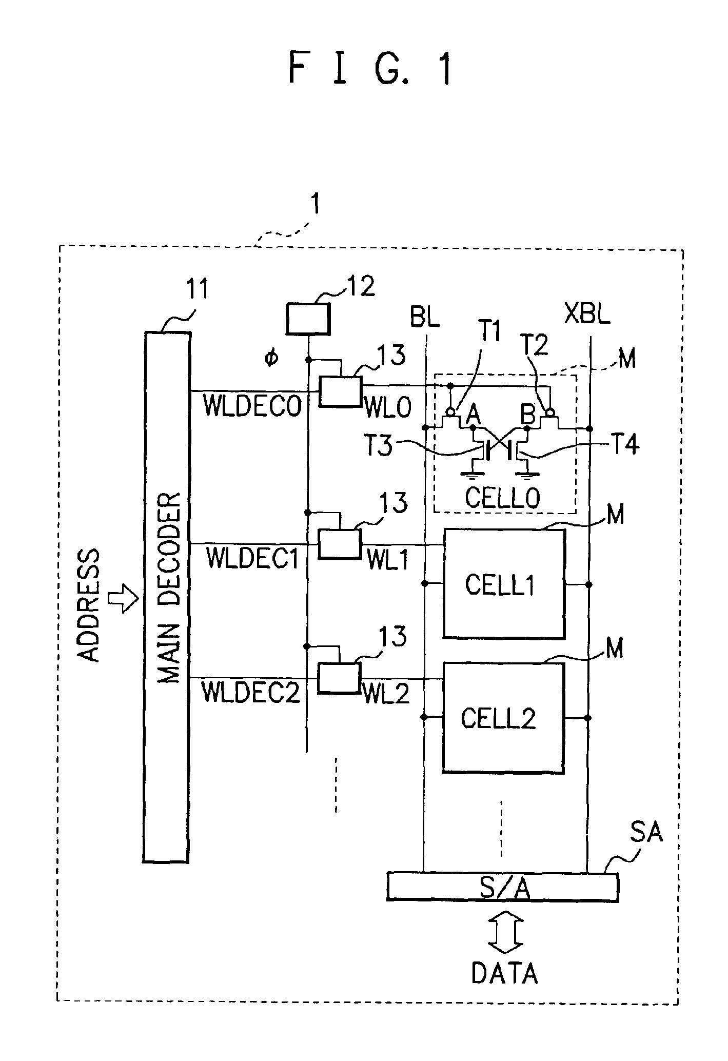
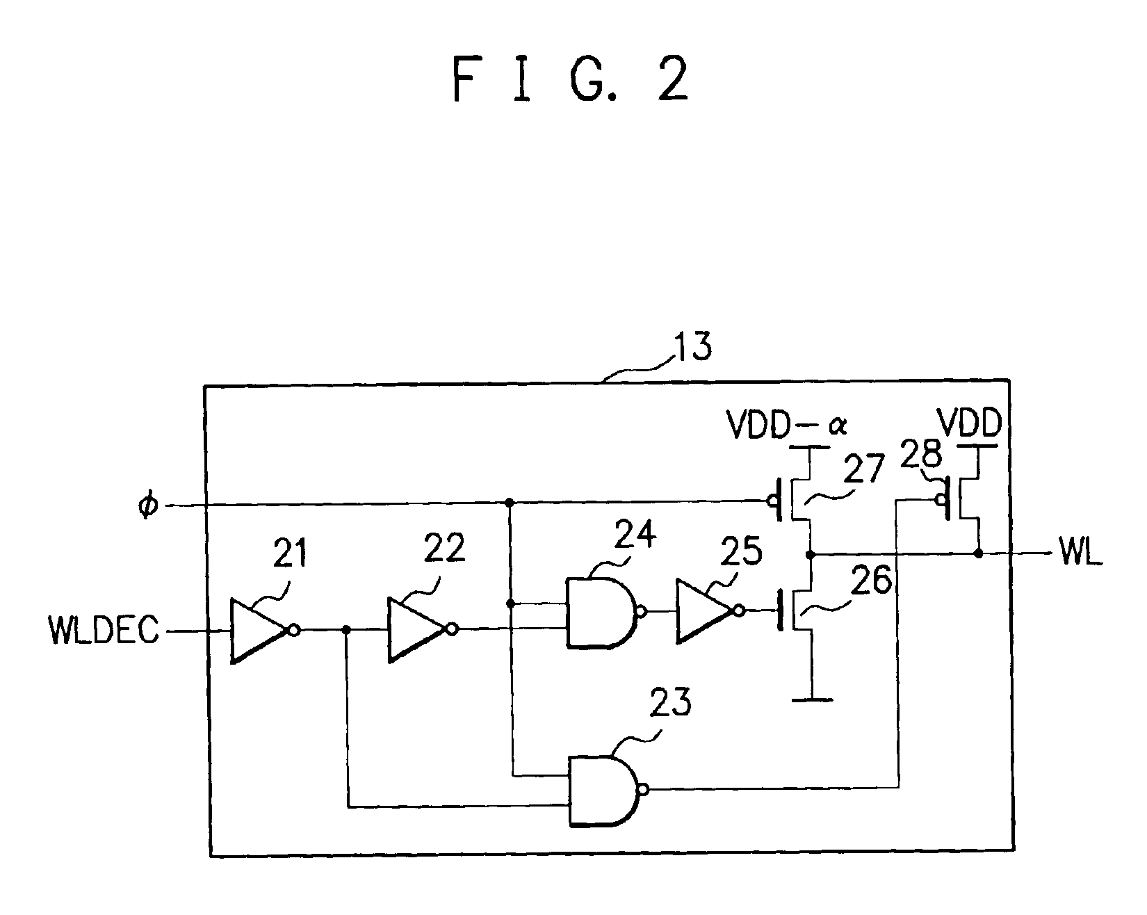
[0043]As the first embodiment, the operation of the word line control circuits 13 will be described assuming that the control signal φ changes to high level in the access mode and low level in the non-access mode in accordance with a change in select signals WLDEC. In the non-access mode of the memory cells M, the word line control circuits 13 change the high-level voltage value of the word lines WL to VDD-α. In the access mode of the specific memory cell M (while the selected word line WL is set to low level), the word line control circuits 13 change the high-level voltage value of the unselected word lines WL to VDD.

second embodiment

[0044]As the second embodiment, the operation of word line control circuits 13 will be described assuming that a control signal φ changes to low level in the access mode and, in the non-access mode, periodically change to high level during a predetermined period. In the non-access mode of the memory cells M, the word line control circuits 13 periodically changes the high-level voltage value of a word lines WL from VDD to VDD-α during a predetermined period. In the access mode of the specific memory cell M (while the selected word line WL is set to low level), the word line control circuits 13 fix the high-level voltage value of the unselected word lines WL to VDD.

[0045]A circuit example of the word line control circuit 13 corresponding to the above-described first embodiment will be described next with reference to the accompanying drawings. The above-described second embodiment will be described later in detail.

[0046]FIG. 2 is a view showing a circuit example of the word line contr...


PUM


Abstract

A word line control circuit controls a high-level voltage value representing that a plurality of word lines are unselected in each of an access mode and non-access mode on the basis of a control signal for controlling the high-level voltage value of the word lines and a control signal output from a main decoder.

Description

CROSS-REFERENCE TO RELATED APPLICATIONS[0001]This application is based upon and claims the benefit of priority from the prior Japanese Patent Application No. 2002-253264, filed on Aug. 30, 2002, the entire contents of which are incorporated herein by reference.BACKGROUND OF THE INVENTION[0002]1. Field of the Invention[0003]The present invention relates to a static semiconductor memory device and a method of controlling the same and, more particularly, to a static semiconductor memory device having memory cells each formed from four transistors and a method of controlling the same.[0004]2. Description of the Related Art[0005]A conventional example of a static semiconductor memory device having memory cells each formed from four transistors is an SRAM (Static Random Access Memory) having 4Tr (transistor) memory cells (the SRAM will be referred to as a 4Tr SRAM hereinafter). FIG. 6 is a view showing the schematic arrangement of the memory cell array of the conventional 4Tr SRAM and a l...

Claims


Application Information

Patent Timeline
IPC IPC(8): G11C11/418G11C8/02G11C11/413G11C11/41
CPCG11C11/418
Inventor ASHIZAWA, TETSUO
Owner SOCIONEXT INC
Why Eureka
Try Eureka