

Semiconductor memory device and data access method for semiconductor memory device
- Summary
- Abstract
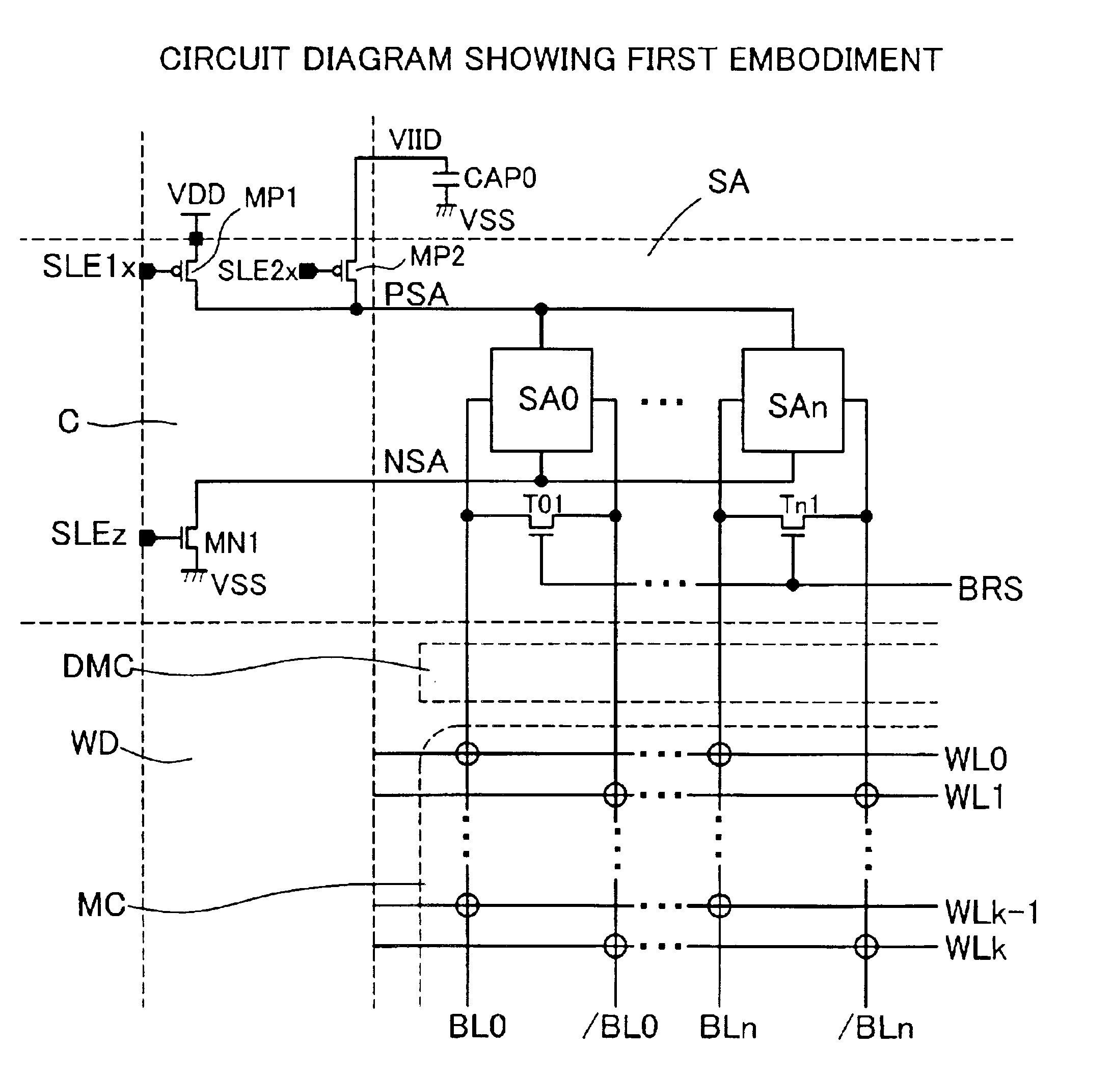
- Description
- Claims
- Application Information
AI Technical Summary
Benefits of technology
Problems solved by technology
Method used
Image

Examples
second embodiment
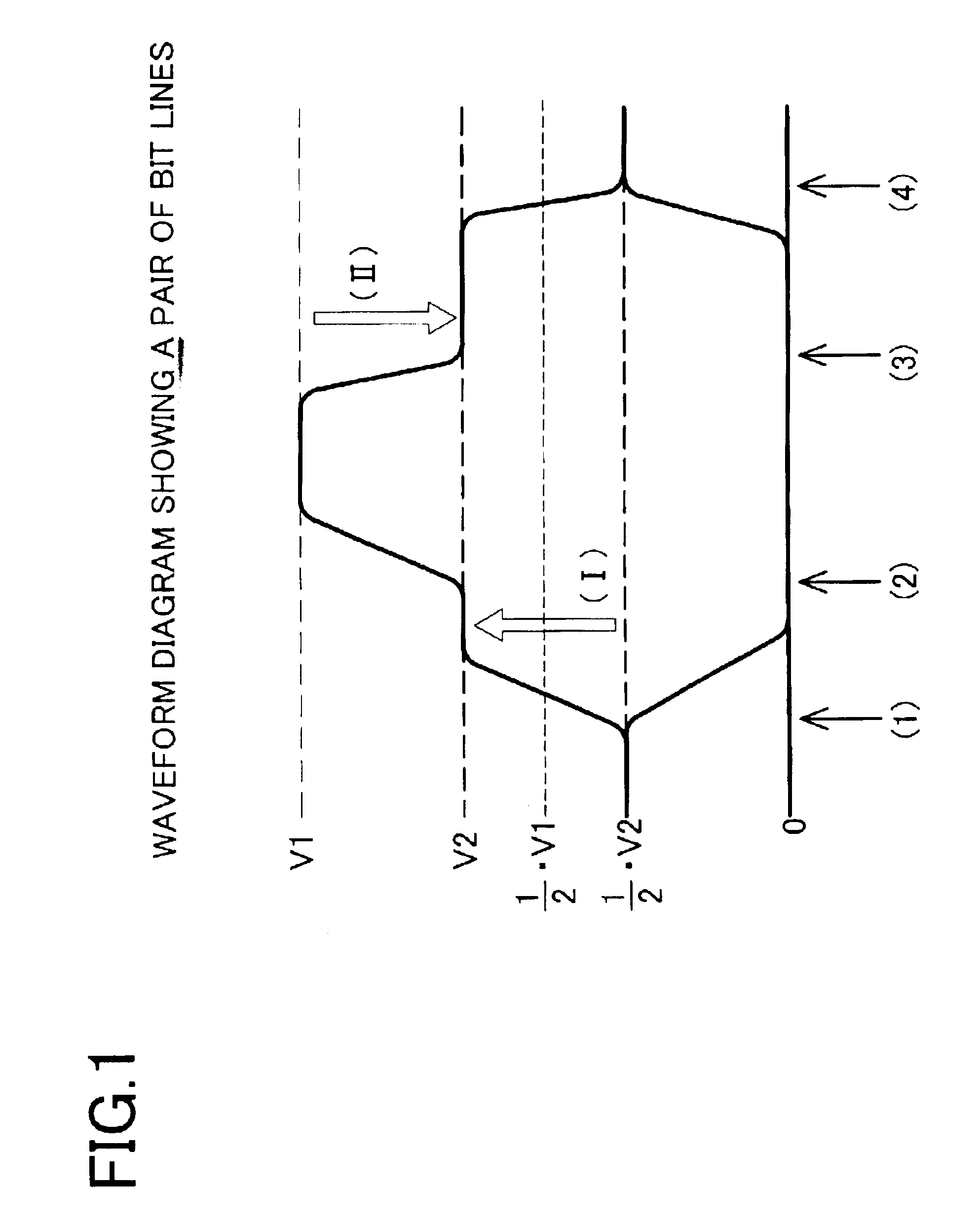
The second embodiment in FIG. 10 is described for the application to the burst read operation. However, the present invention can be applied to a general page operation in the same manner if it is a successive operation. The burst operation and the page operation differ in that a column address is changed sequentially or at random. The equalize operation in the first stage on the bit line pairs (BL, / BL) are the same in both operation modes.
Furthermore, the present invention can be applied to a successive write operation. In this case, a series of data to be successively written may be captured by data temporally holding means such as a buffer circuit within the device when or after the initiation of the active operation (ACTV), which is the initial stage of the successive operation mode. Thus, data is captured sequentially from the data temporally holding means in the successive write cycle, and data is written. If the word line WL is deactivated when the last bit has completely wri...
PUM
 Abstract
Description
Claims
Application Information