Polymer optical waveguides on polymer substrates

Inactive Publication Date: 2005-07-12
PHOTON
View PDF23 Cites 17 Cited by
  • Summary
  • Abstract
  • Description
  • Claims
  • Application Information

AI Technical Summary

Problems solved by technology

The mismatch of CTE between the silicon substrate and the polymer waveguide claddings and core can cause polymer film cracking and stress build-up in the polymer layers.
These effec

Method used


Image

  • Polymer optical waveguides on polymer substrates
  • Polymer optical waveguides on polymer substrates
  • Polymer optical waveguides on polymer substrates

Examples


Embodiment Construction

[0018]In the drawings, like numerals indicate like elements throughout. U.S. Pat. No. 6,603,917 B2, filed on even date, which is owned by the assignee of the present invention, is incorporated herein by reference in its entirety. As used herein, the term “element” is defined to mean ions, atoms, isotopes, and species of atoms of the Periodic Table.

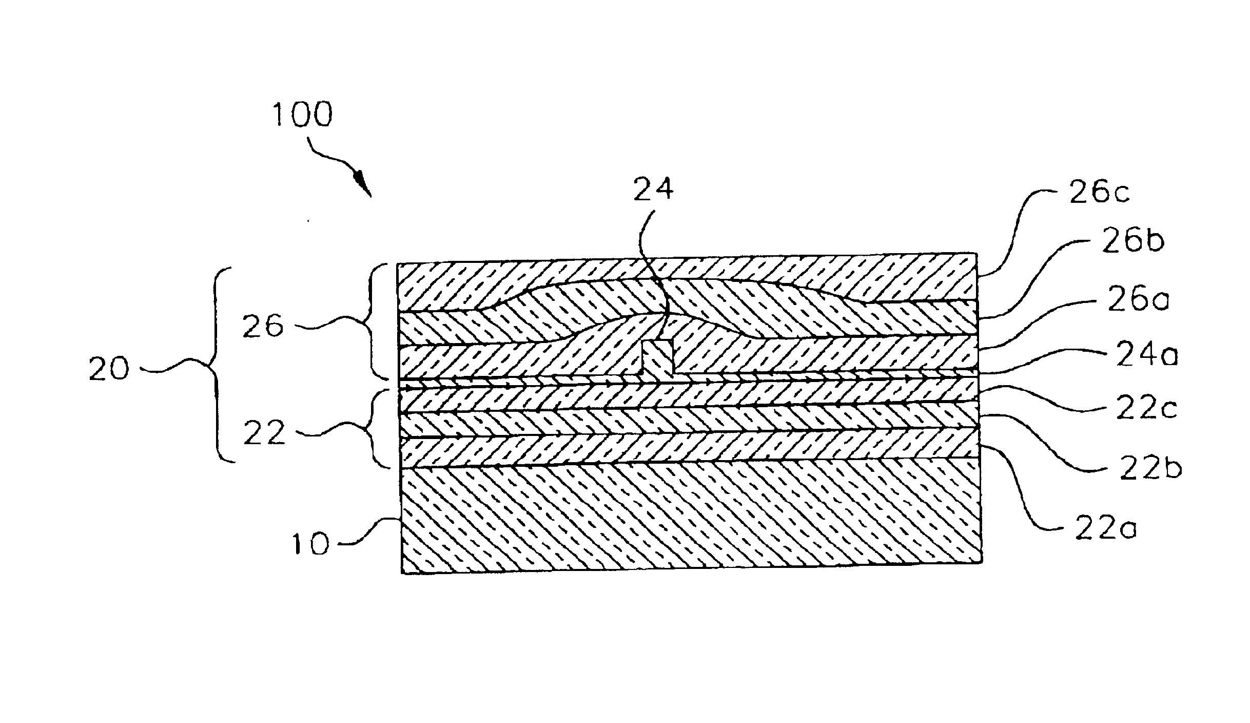
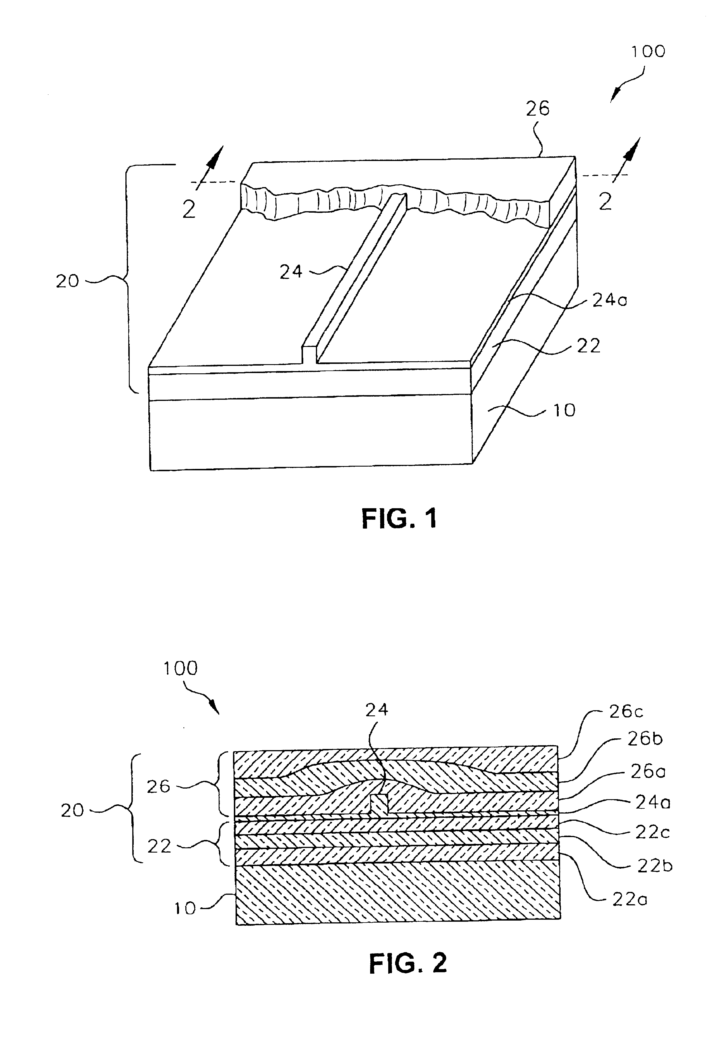
[0019]Referring to FIGS. 1 and 2, an optical waveguide assembly 100 is comprised of a polymer substrate 10 with a polymer optical waveguide 20 disposed on the substrate 10. The waveguide 20 is comprised of a lower cladding 22, a core 24 disposed on at least a portion of the lower cladding 22, and an upper cladding 26 disposed on the core 24 and a remaining portion of the lower cladding 22. Preferably, the lower cladding 22, the core 24, and the upper cladding 26 are all polymers, and more preferably, all perhalogenated polymers, and most preferably, perfluoropolymers.

[0020]Preferably, the substrate 10 is from the group consisting of polyca...


PUM


Abstract

An optical waveguide is provided. The optical waveguide includes a polymer substrate and a lower cladding disposed on the substrate. The lower cladding is a first perhalogenated polymer. The optical waveguide also includes a core disposed on at least a portion of the lower cladding. A method of manufacturing the optical waveguide is also provided.

Description

FIELD OF THE INVENTION[0001]The present invention relates to polymer optical waveguides disposed on polymer substrates, and more specifically, to perfluorinated polymer optical waveguides.BACKGROUND OF THE INVENTION[0002]Optical waveguides can be formed in polymers by using a core polymer and a cladding polymer with the core polymer refractive index slightly higher than that of the cladding polymer in the near infrared region of the third optical telecommunication wavelength window (around 1550 nm). In order to form useful optical waveguide devices such as integrated splitters, couplers, arrayed waveguide gratings, and optical waveguide amplifiers, it is essential to have stable and low loss optical waveguides. The optical loss, or attenuation of an optical waveguide, originates primarily from two sources: 1) optical absorption by the core and cladding material and 2) optical signal scattering from the waveguide.[0003]A general approach to making polymer optical waveguides is to dis...

Claims


Application Information

Patent Timeline
IPC IPC(8): G02B6/13G02B6/138G02B6/12H01S3/10
CPCG02B6/138G02B2006/121G02B2006/12107G02B2006/12147G02B2006/1215
Inventor GAO, RENYUANBITTING, DONALD S.MININNI, ROBERT M.NORWOOD, ROBERT A.TAKAYAMA, KAZUYAGARITO, ANTHONY F.
Owner PHOTON
Why Eureka
Try Eureka