Method of and apparatus for integrating flash EPROM and SRAM cells on a common substrate

a technology of flash eprom and sram cells, applied in the direction of electrical apparatus, basic electric elements, semiconductor devices, etc., can solve the problems of ineffective use of active devices or isolation, occupying active areas, and unable to isolate effectively

Inactive Publication Date: 2005-07-26
ACACIA PATENT ACQUISITION
View PDF23 Cites 8 Cited by
  • Summary
  • Abstract
  • Description
  • Claims
  • Application Information

AI Technical Summary

Benefits of technology

[0011]A system for and a method of integrating SRAM cells and flash EPROM cells onto a single silicon substrate includes an area on the silicon substrate where a local oxidation of silicon (LOCOS) isolation technique is implemented and another area on the same silicon substrate where a shallow trench isolation (STI) technique is implemented. Further, this system and method also include flash EPROM cells implemented within the area of the substrate utilizing the LOCOS isolation technique and SRAM cells implemented within the area of the substrate utilizing the STI technique. Preferably, the LOCOS isolation technique is first implemented to define a flash area of the silicon substrate on which the flash EPROM cell is implemented. Before the LOCOS isolation technique is implemented, an SRAM area is masked. After the LOCOS isolation technique has been fully implemented, the flash area is then preferably masked and the STI technique is implemented in order to define the SRAM area of the silicon substrate on which the SRAM cell is implemented. After the STI technique is implemented, the flash EPROM and the SRAM cells are preferably formed. Thus, the SRAM cells and the flash EPROM cells are both implemented on the common silicon substrate, but yet are appropriately isolated from each other, as well as from other additional devices which may be further implemented on the same silicon substrate, while providing the advantages of respective isolation schemes for the two cells.

Problems solved by technology

One major limitation of LOCOS isolation techniques is the problem of active area encroachment which occurs during the growth of the field oxide regions 25.
This area is not flat and, accordingly, cannot be used effectively for active devices or isolation.
Furthermore, the LOCOS isolation technique requires a larger amount of space for device packing compared to other isolation techniques.
STI techniques have a drawback of not being compatible with higher voltages and endurance requirements.
If the SRAM device and the flash EPROM are implemented separately and piggybacked, then signals sent between the SRAM device and the flash EPROM must exit the originating device and enter the receiving device, leading to possible signal delays.
Stacking flash EPROM and SRAM devices within a package may also cause package reliability problems.

Method used


Image

  • Method of and apparatus for integrating flash EPROM and SRAM cells on a common substrate
  • Method of and apparatus for integrating flash EPROM and SRAM cells on a common substrate
  • Method of and apparatus for integrating flash EPROM and SRAM cells on a common substrate

Examples


Embodiment Construction

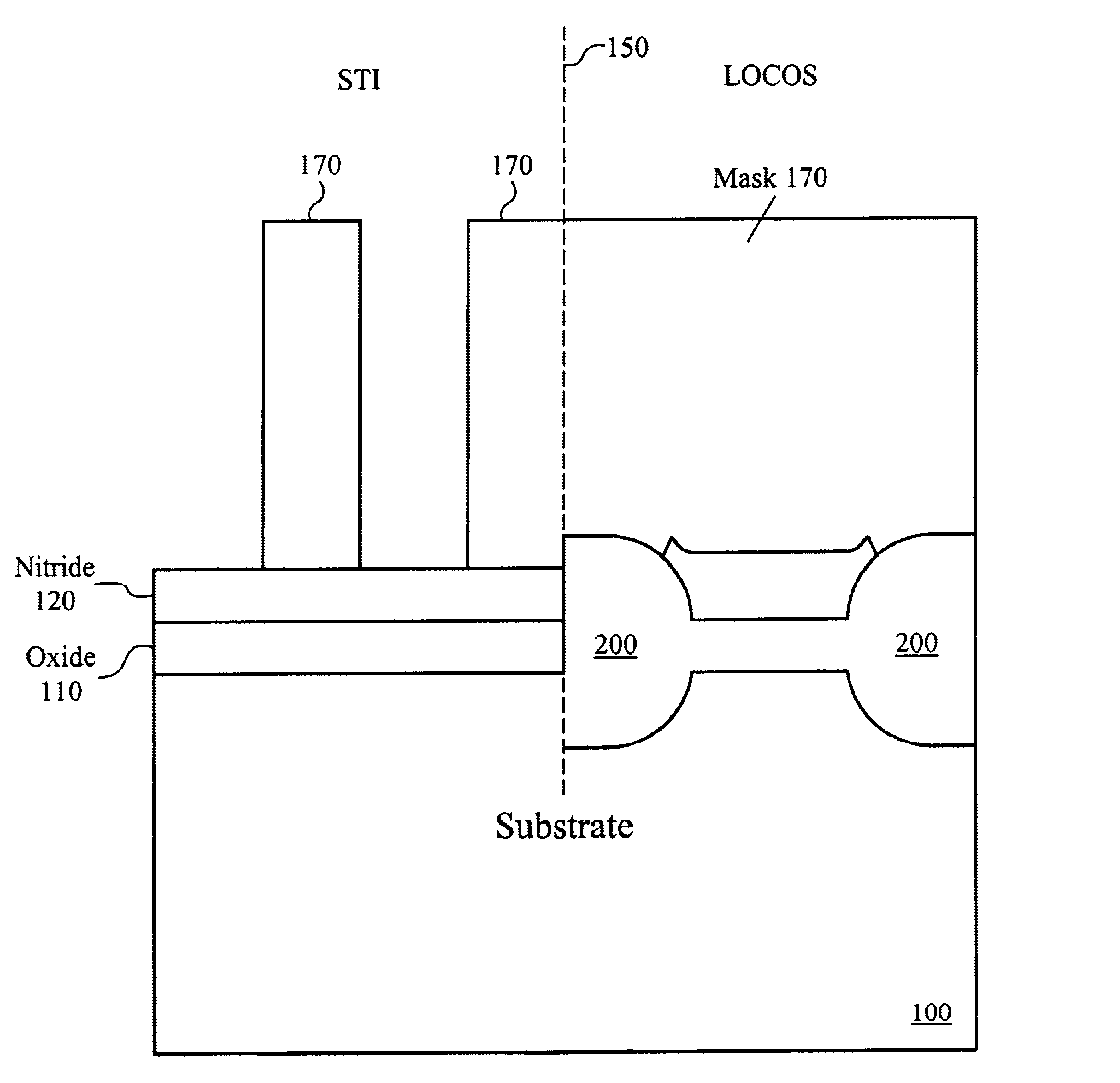
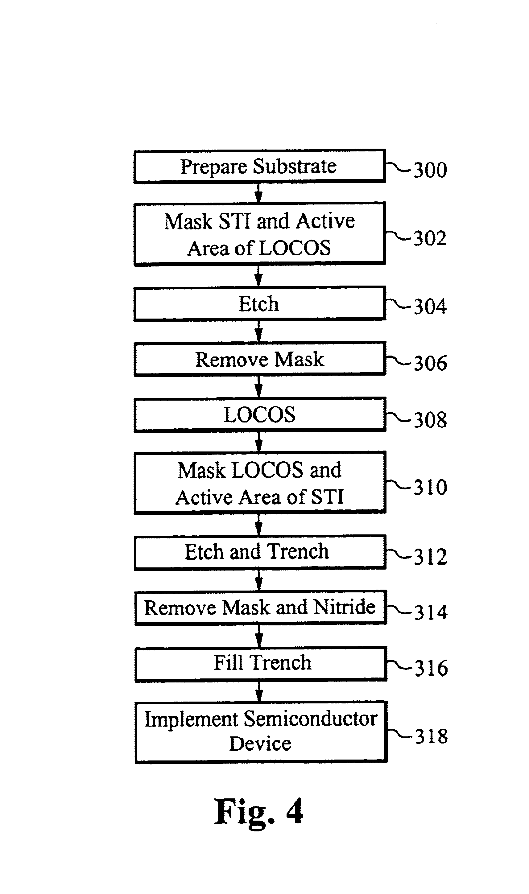
[0026]A system for and a method of integrating SRAM and flash EPROM cells on a common silicon substrate using appropriate isolation techniques allows the present invention to reduce the package size, increase durability and reliability of the semiconductor device and increase communication speed and accuracy between the SRAM and flash EPROM cells. The present invention allows the STI process and the LOCOS process to be implemented on the same silicon substrate. The STI process is optimized for utilization with the SRAM cells. The STI process allows a greater density of cells to be implemented within an area of the silicon substrate than does the LOCOS process. The LOCOS process is optimized for utilization with the flash EPROM cells. The LOCOS process is capable of effectively isolating areas in which larger voltages are utilized than the STI process. By implementing the STI process in locations on the common silicon substrate where the SRAM cells are utilized and by implementing th...


PUM


Abstract

A system for and a method of integrating SRAM cells and flash EPROM cells onto a single silicon substrate includes an area on the silicon substrate where a local oxidation of silicon (LOCOS) isolation technique is implemented and another area on the same silicon substrate where a shallow trench isolation (STI) technique is implemented. Further, this system and method also include flash EPROM cells implemented within the area of the substrate utilizing the LOCOS isolation technique and SRAM cells implemented within the area of the substrate utilizing the STI technique. Preferably, the LOCOS isolation technique is first implemented to define a flash area of the silicon substrate on which the flash EPROM cell is implemented. Before the LOCOS isolation technique is implemented, an SRAM area is masked. After the LOCOS isolation technique has been fully implemented, the flash area is then preferably masked and the STI technique is implemented in order to define the SRAM area of the silicon substrate on which the SRAM cell is implemented. After the STI technique is implemented, the flash EPROM and the SRAM cells are preferably formed. Thus, the SRAM cells and the flash EPROM cells are both implemented on the common silicon substrate, but yet are appropriately isolated from each other, as well as from other additional devices which may be further implemented on the same silicon substrate, while providing the advantages of respective isolation schemes for the two cells.

Description

[0001]This is a divisional of U.S. patent application Ser. No. 09 / 3 15,599, filed May 20, 1999, the contents of which are hereby incorporated by reference.FIELD OF THE INVENTION[0002]The present invention generally relates to the field of semiconductor memory structures. More particularly, the present invention relates to a method for integrating a nonvolatile erasable programmable read-only flash memory (flash EPROM) and a static random access memory (SRAM) on a common substrate.BACKGROUND OF THE INVENTION[0003]Flash EPROMS are non-volatile electrically erasable integrated circuit memory devices. Flash EPROMS utilize hot-electron injection for programming and Fowler-Nordheim tunnelling for erase. A cross-section of a conventional flash EPROM is illustrated in FIG. 1. The flash memory cell 10 is typically fabricated in a substrate 20 of p-type silicon with a source region 14 optimized for the erase condition and a drain region 16 optimized for hot-electron programming. The flash mem...

Claims


Application Information

Patent Timeline
Patent Type & Authority Patents(United States)
IPC IPC(8): H01L29/00H01L21/70H01L21/8238H01L21/762H01L21/8239H01L21/8244H01L21/8247H01L27/105H01L27/11H01L27/115
CPCH01L21/76202H01L21/76224H01L27/105H01L27/11H01L27/1116H01L27/11517H01L27/11526H01L27/1052H10B99/00H10B10/18H10B10/00H10B41/00H10B41/40
Inventor SHRIVASTAVA, RITU
Owner ACACIA PATENT ACQUISITION
Why Eureka
Try Eureka