Ultraviolet erasable semiconductor memory device

a technology of ultraviolet erasing and memory devices, which is applied in the direction of digital storage, instruments, transistors, etc., can solve the problems of difficult to confirm whether the data is erased, difficult that a user rewrites the initial data and stores the desired data,

Active Publication Date: 2007-07-10
SEMICON COMPONENTS IND LLC
View PDF6 Cites 5 Cited by
  • Summary
  • Abstract
  • Description
  • Claims
  • Application Information

AI Technical Summary

Benefits of technology

[0009]The present invention solves the above-described problems and has an object of preventing an output of a differential amplifier from being unstable in an initialized state and, then, facilitating confirmation of the initialized state at a user's side in an ultraviolet erasable semiconductor memory device comprising a memory cell comprising two MOSFETs and detecting a difference of data signal current therebetween by using the differential amplifier.

Problems solved by technology

However, in a state in which data is erased by ultraviolet ray irradiation, that is, in an initialized state, since Vts of two MOSFETs are same with each other, a given value can not be obtained in an output of the differential amplifier.
For this account, there is caused an inconvenience in that it is difficult to confirm whether the data is erased or not (or whether used or not used).
However, in order to erase the data in the EPROM, it is necessary to irradiate the ultraviolet ray thereon and, once the initializing data is written, it is difficult that a user rewrites the initial data and, then, stores a desired data.
Therefore, the above-described inconvenience is an intrinsic problem in the ultraviolet erasable semiconductor memory device.

Method used


Image

  • Ultraviolet erasable semiconductor memory device
  • Ultraviolet erasable semiconductor memory device
  • Ultraviolet erasable semiconductor memory device

Examples


Embodiment Construction

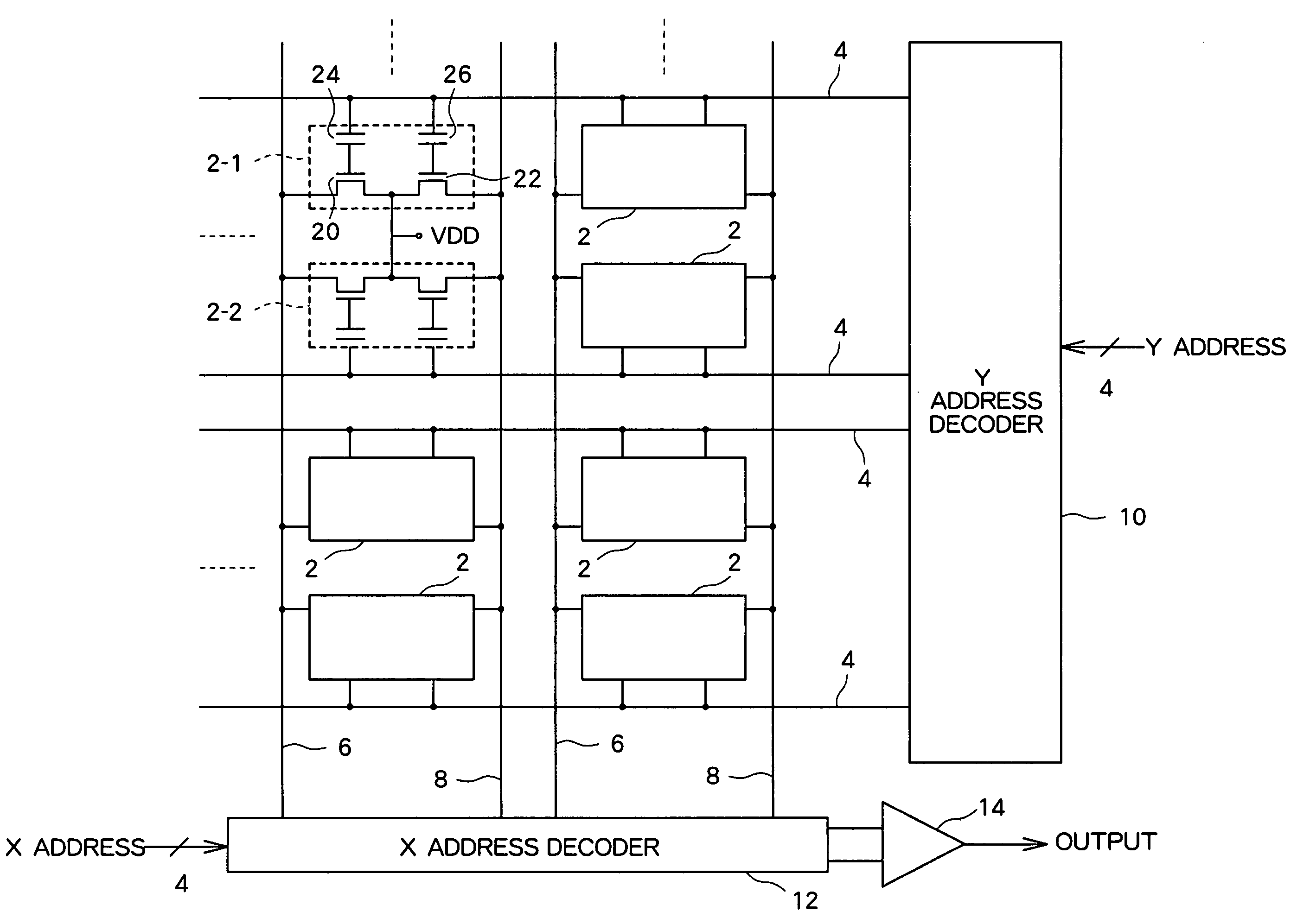
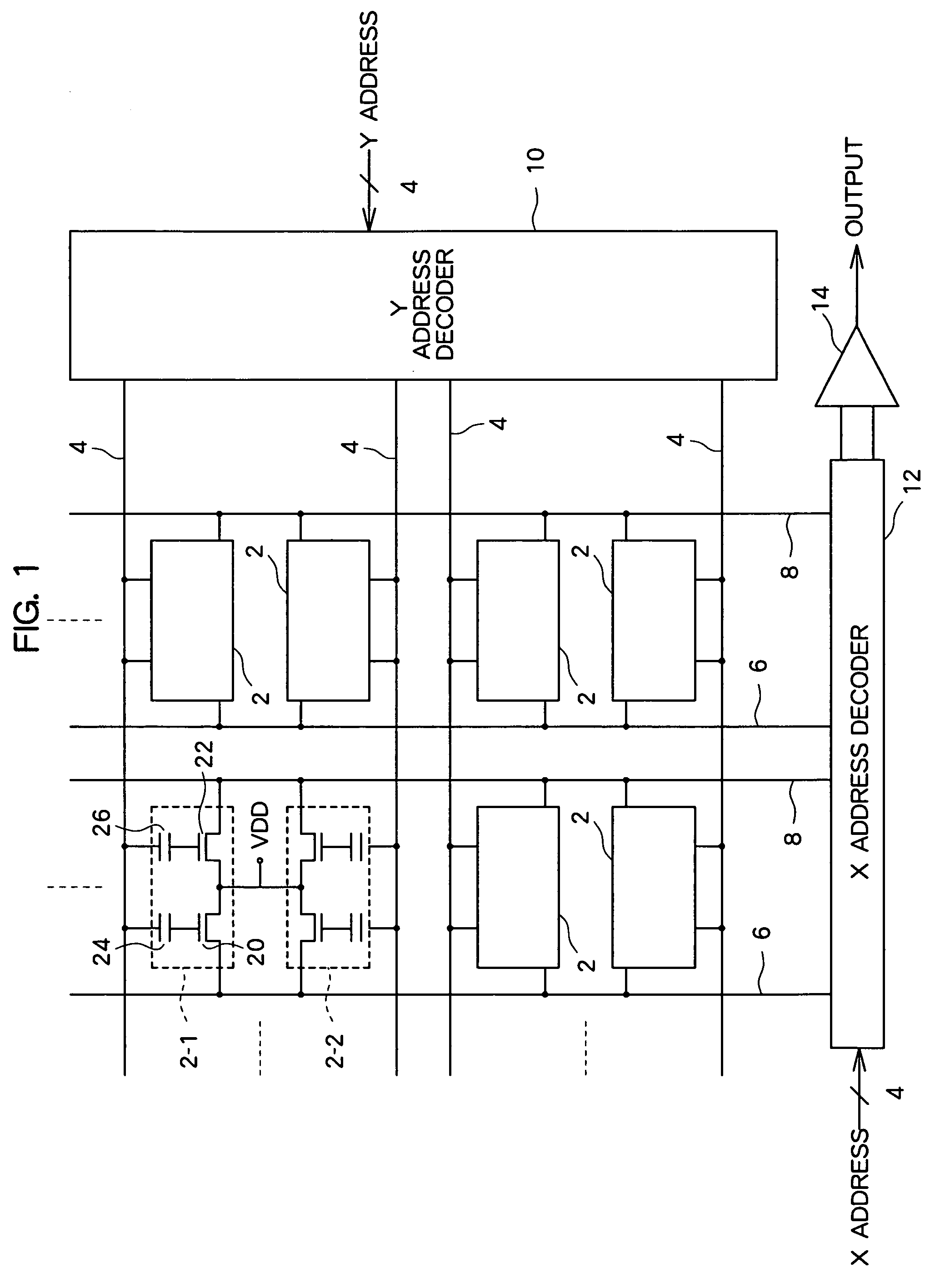
[0013]Firstly, a fundamental aspect of an ultraviolet erasable semiconductor memory device which is a preferred embodiment according to the present invention is outlined.

[0014]As a fundamental constitution, the ultraviolet erasable semiconductor memory device according to an embodiment of the present invention comprises a memory cell comprising a pair of transistors of field effect type to be selected by a common selection signal and a differential amplifier which reads out data recorded in the memory cell based on a magnitude relation between respective data signal currents drawn out from the pair of transistors, in which the pair of transistors have therebetween a predetermined signal current difference between respective data signal currents in a state in which the data in the memory cell is erased.

[0015]In the present memory device, a pair of transistors provided in a memory cell are set in a state in which channel currents (data signal currents) thereof are different from each ...


PUM


Abstract

Each memory cell of an EPROM contains two MOSFETs and a data of each memory cell is read out by detecting a current difference between the two MOSFETs by using a differential amplifier. In such constitution as described above, even when the data is erased by irradiating an ultraviolet ray, a stable output of the differential amplifier can be obtained and, therefore, confirmation of an initialized state can be facilitated. Specifically, a channel width WA of one of the two MOSFETs constituting the memory cell is formed narrower than a channel width WB of the other. By such arrangement as described above, in an initialized state in which the ultraviolet ray is irradiated, a data signal current value IHA of the MOSFET having the channel width WA becomes smaller than a data signal current value IHB flowing in the MOSFET having the channel width WB. Accordingly, the output of the differential amplifier is fixed in accordance with a current magnitude relation of IHA<IHB, to thereby define a data “0”. On the other hand, in writing a data “1”, charges are injected in a floating gate electrode of the MOSFET having the channel width WB to raise a threshold voltage Vt and, then, the MOSFET is set in an “off” state.

Description

CROSS-REFERENCE TO RELATED APPLICATIONS[0001]The priority application Number JP2004-050362 filed Feb. 25, 2004, upon which this patent application is based is hereby incorporated by reference.FIELD OF THE INVENTION[0002]The present invention relates to an ultraviolet erasable semiconductor memory device capable of erasing stored data by irradiating an ultraviolet ray.BACKGROUND OF THE INVENTION[0003]In semiconductor memory devices, there is an EPROM (Erasable Programmable Read Only Memory) which can not only electrically write data but also erase the data by irradiating an ultraviolet ray on a transistor holding the data. Ordinarily, a semiconductor has memory cells which each store 1-bit data are arrayed in a matrix and can perform a data writing operation and a data reading operation for a memory cell in a designated position, for example, by designating a row and a column by using an address decoder. For example, a word line of each memory cell is connected to a Y address decoder...

Claims


Application Information

Patent Timeline
Patent Type & Authority Patents(United States)
IPC IPC(8): G11C16/04G11C17/00G11C5/00G11C8/00G11C11/34G11C11/42G11C16/00G11C16/06G11C16/18H01L21/8247H01L27/10H01L27/115H01L29/78H01L29/788H01L29/792
CPCG11C16/18G11C8/00H10B41/00
Inventor KUMAGAI, YUKIHISA
Owner SEMICON COMPONENTS IND LLC
Why Eureka
Try Eureka