Electronic memory having impedance-matched sensing

a technology of impedance matching and electronic memory, applied in the field of semiconductor memory, can solve the problems of affecting the accuracy of data sensing, so as to achieve the same impedance characteristics and accurate data sensing

Active Publication Date: 2005-02-17
PROMOS TECH INC
View PDF8 Cites 5 Cited by
  • Summary
  • Abstract
  • Description
  • Claims
  • Application Information

AI Technical Summary

Benefits of technology

[0010] The present invention furnishes such a data sensing arrangement for an electronic memory having global bit lines that fully traverse the memory and local bit lines that only partially traverse the memory. The sensing arrangement of the invention employs impedance matching to achieve highly accurate data sensing with low sensitivity to noise. Selection / connection circuitry appropriately interconnects different memory portions, including the local and global bit lines, to implement the impedance matching in a highly efficient manner. The memory is preferably a flash EPROM whose memory cells are formed with floating-gate FETs of the split-gate type. Consequently, the present memory system is typically not subjected to cell overerasure difficulties and does not require measures, such as soft programming, to overcome overerasure.
[0016] By operating the memory so that none of the memory cells along the local bit lines associated with the reference global bit line is selected, the sense amplifier reads a selected one of the cells along the selected local bit line. Due to the architecture of the memory, the reference local bit line, the reference global bit line, and the data line connected to the reference global bit line respectively have largely the same impedance characteristics as the local bit line, the global bit line, and the data line for the cell being read. Impedance matching thereby occurs at the input terminals of the sense amplifier to produce highly accurate data sensing.
[0018] The reference circuitry is achieved by providing the memory with selection / connection circuitry that, in addition to having the capability for selecting each local bit line, is operable (a) to electrically connect each selected local bit line in each memory section of each of the section columns to the sense amplifier's data input terminal by way of (a1) the global bit line for the selected local bit line and (a2) the data line for the selected local bit line and (b) to largely simultaneously electrically connect a reference one of the global bit lines for another of the section columns to the amplifier's reference input terminal by way of the data line for the reference global bit line. By again operating the memory so that none of the cells along the local bit lines associated with the reference global bit line is selected, the sense amplifier reads a selected cell along the selected local bit line. Appropriately configuring the reference bit line, including arranging for the number of reference memory cells to be the same as the number of memory cells in each cell column of each memory section, enables the reference bit line, the reference global bit line, and the data line connected to the reference global bit line to respectively have largely the same impedance characteristics as the local bit line, the global bit line, and the data line for the cell being read. The resultant impedance matching at the amplifier's input terminals produces accurate data sensing.

Problems solved by technology

The resultant increased impedance is disadvantageous.
However, if a read operation were performed on one memory section 20 or 22 in FIG. 1 at a time when the other section 22 or 20 contains an overerased cell, i.e., during erasure and / or prior to “soft” programming, the current flowing through the overerased cell could severely damage the sensing accuracy.
This is cumbersome because it requires substantial circuitry to perform the array switching.

Method used


Image

  • Electronic memory having impedance-matched sensing
  • Electronic memory having impedance-matched sensing
  • Electronic memory having impedance-matched sensing

Examples


Embodiment Construction

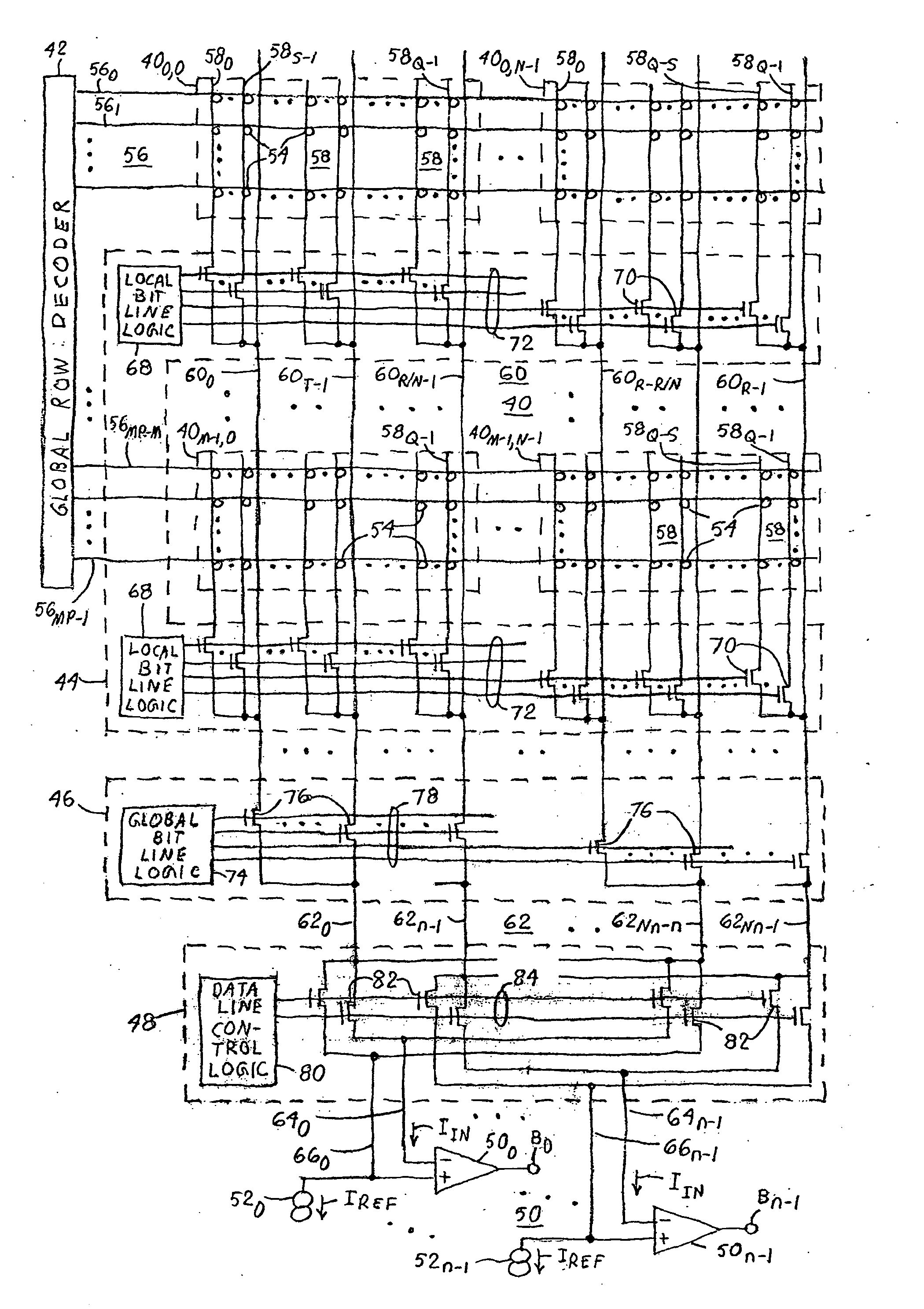
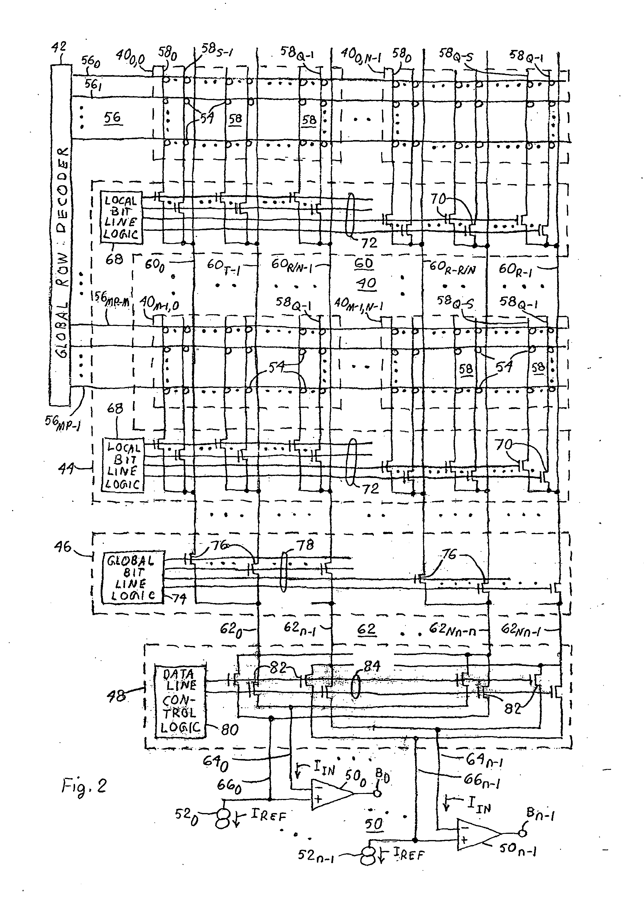
[0030] In the following description, elements that fall into sequences or are grouped into two-dimensional arrays are generally collectively labeled by reference symbols without subscripts. An element's position in a sequence or two-dimensional array is indicated by using the collective reference symbol for the element followed by a subscript position indicator. Each of subscripts “i”, “j”, and “k” is a running integer for an arbitrary position in a sequence or two-dimensional array. Symbols “M”, “N”, “P”, “Q”, “R”, “S”, and “T” are fixed integers.

[0031] As used below, “connection” means an electrical connection except as otherwise indicated. Similarly, “line” means an electrical line or conductor. All FETs described below are n-channel insulated-gate FETs except as otherwise indicated.

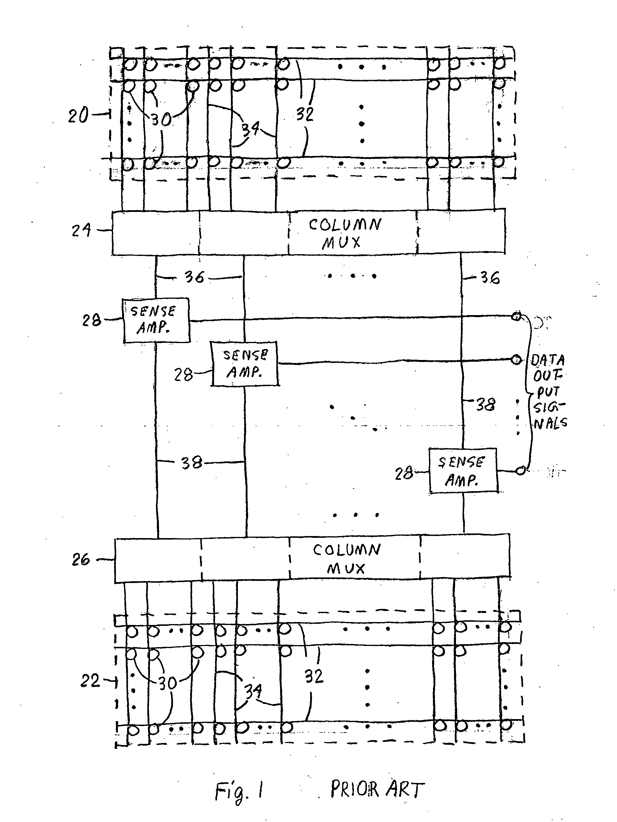
[0032]FIG. 2 illustrates a memory configured according to the invention for achieving impedance-matched data sensing. The memory of FIG. 2 contains a group of largely identical local storage memory ...


PUM


Abstract

An electronic memory, typically a flash EPROM, contains an array of memory sections (40), each containing an array of memory cells (54). Global bit lines (60) fully traverse the memory. Local bit lines (58) partially traverse the memory. Data stored in the memory is sensed with an arrangement that utilizes impedance matching to achieve high sensing accuracy with low noise sensitivity. The impedance matching may be provided solely from the sections and lines of the memory or partially from a separate reference memory section (102) that contains reference memory cells (104).

Description

FIELD OF USE [0001] This invention relates to semiconductor memories, especially erasable programmable read-only memories (“EPROMs”) of the flash-erasable type. BACKGROUND ART [0002] Semiconductor memories are formed with memory cells that store bits of data. The memory cells are normally very small. As a result, cell data signals that indicate the states of the stored data are electrically small and need to be amplified. Devices commonly referred to as sense amplifiers provide the amplification. A sense amplifier typically amplifies the difference between a data signal received at one input terminal and a reference signal received at another input terminal. Because the cell data signals are small, sense amplifiers must be highly sensitive to correctly read the stored data. [0003] One way to enhance the sensitivity of a sense amplifier is to employ a balanced sensing arrangement that takes advantage of the largely matching impedance characteristics of portions of the circuitry used ...

Claims


Application Information

Patent Timeline
Patent Type & Authority Applications(United States)
IPC IPC(8): G11C7/06G11C7/14G11C7/18G11C16/28
CPCG11C7/06G11C16/28G11C7/18G11C7/14
Inventor KIM, JONGJUN
Owner PROMOS TECH INC
Why Eureka
Try Eureka