Inductor element

a technology of inductor elements and elements, applied in the direction of semiconductor devices, solid-state devices, inductances, etc., can solve the problems of difficult to form a high-frequency circuit including the inductor element on a semiconductor substrate, and the inductor element cannot effectively function as the inductor element, so as to achieve the effect of effective function

Inactive Publication Date: 2005-07-26
RICOH KK
View PDF7 Cites 19 Cited by
  • Summary
  • Abstract
  • Description
  • Claims
  • Application Information

AI Technical Summary

Benefits of technology

[0003]The present invention is achieved in view of such a point. Its object is to provide an inductor element that effectively functions even if the inductor element is formed on a substrate.

Problems solved by technology

Nevertheless, since eddy currents are induced on the front side of the semiconductor substrate by this magnetic flux to cancel effective magnetic flux, there is such a problem that doesn't effectively function as the inductor element.
In particular, since the higher a frequency of a signal which flows in the inductor element becomes, the more remarkable this inclination becomes, and consequently it is difficult to form a high frequency circuit including the inductor element on a semiconductor substrate.

Method used


Image

  • Inductor element
  • Inductor element
  • Inductor element

Examples


Embodiment Construction

[0020]Hereafter, an inductor element according to an embodiment where the present invention is applied will be specifically described with referring to drawings.

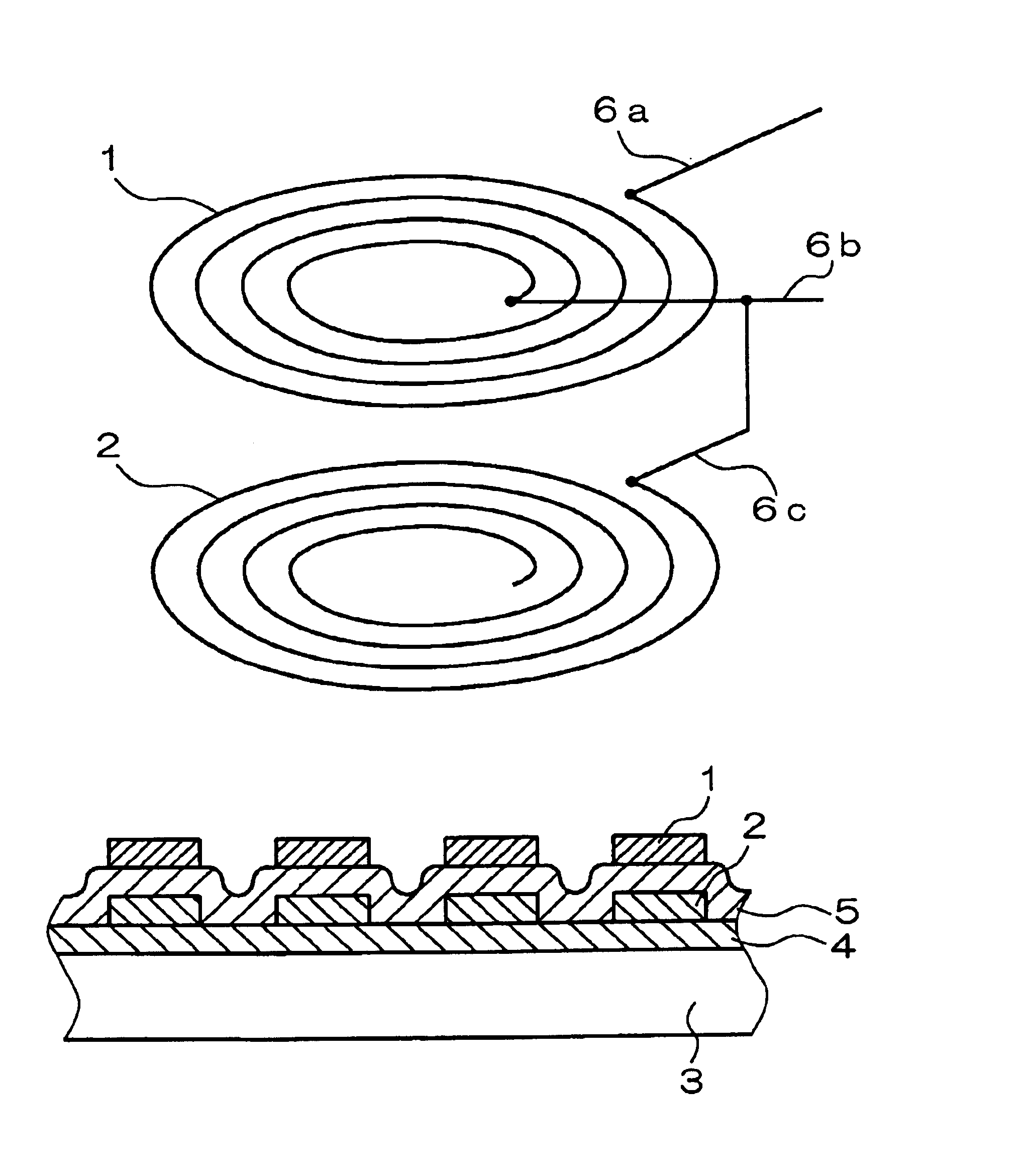
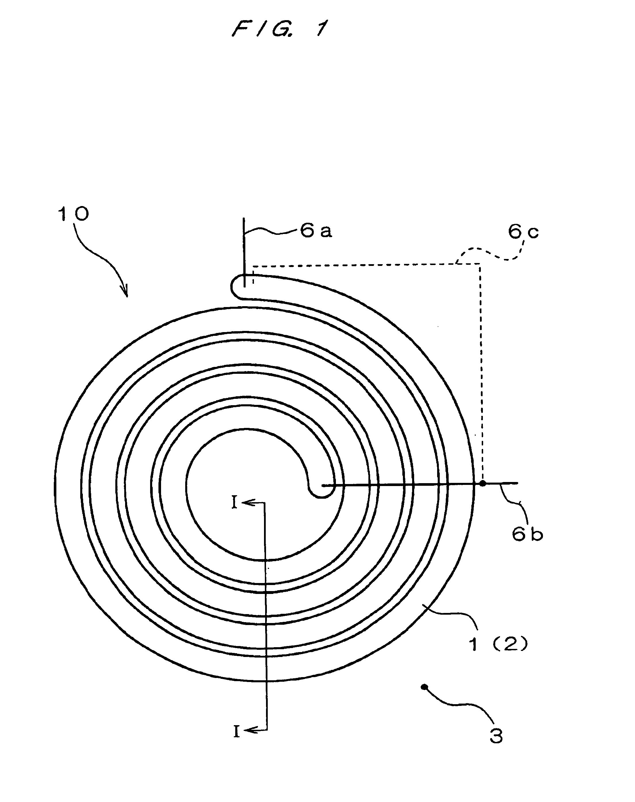
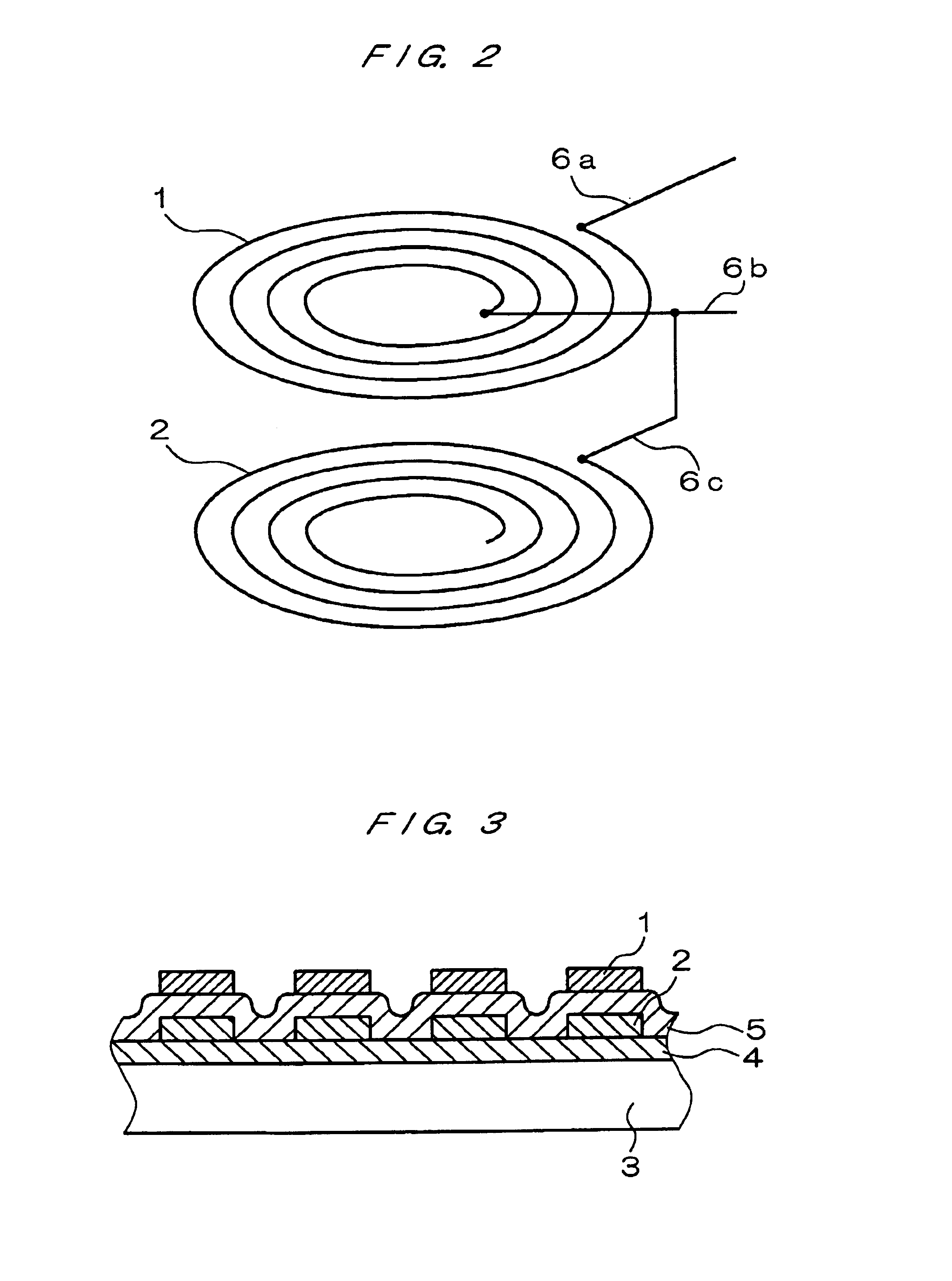
[0021]FIG. 1 is a schematic diagram showing a planar structure of an inductor element according to this embodiment that is formed on a substrate. An inductor element 10 according to this embodiment has two conductors 1 and 2 that have spiral shapes and are formed in the front side of a semiconductor substrate 3.

[0022]These two conductors 1 and 2 have substantially the same shape. As shown in FIG. 1, when viewed from the front side of the semiconductor substrate 3, they are formed so that the conductor 1, which becomes an upper layer, and another conductor 2, which becomes a lower layer, are formed by being superimposed one on the other substantially exactly. Each of the conductors 1 and 2 is formed of a thin film of metal such as aluminum or gold, or semiconductor material such as poly silicon.

[0023]FIG. 2 is a schematic dia...


PUM

PropertyMeasurementUnit
dielectric constantaaaaaaaaaa
oscillation frequencyaaaaaaaaaa

Abstract

An inductor element 10 effectively functions even when formed on a substrate and comprises two upper and lower conductors 1, 2 spirally formed on the front side of a semiconductor substrate 3. The conductors 1, 2 have substantially the same shape. When viewed from the above of the front side of the substrate 3, the two conductors 1, 2 are superposed one on the other almost exactly. Lead wires 6a, 6b are connected to the outer end (outer peripheral end) and the inner end (center end) of the conductor 1, respectively. The outer end of the conductor 1 is connected to the inner end of the conductor 2 through a connection wire 6c. The conductor 1 functions as an inductor conductor and is connected to a circuit provided on the semiconductor substrate 3 through the lead wires 6a, 6b.

Description

TECHNICAL FIELD[0001]The present invention relates to an inductor element that can be formed on various kinds of substrates such as a semiconductor substrate.BACKGROUND ART[0002]There is known such a semiconductor circuit that forms a spiral pattern on a semiconductor substrate by using thin film forming technique, and uses this pattern as an inductor element. When current flows in such an inductor element that is formed on a semiconductor substrate, magnetic flux is generated in the direction perpendicular to a spiral pattern. Nevertheless, since eddy currents are induced on the front side of the semiconductor substrate by this magnetic flux to cancel effective magnetic flux, there is such a problem that doesn't effectively function as the inductor element. In particular, since the higher a frequency of a signal which flows in the inductor element becomes, the more remarkable this inclination becomes, and consequently it is difficult to form a high frequency circuit including the i...

Claims


Application Information

Patent Timeline
Patent Type & Authority Patents(United States)
IPC IPC(8): H01F17/00H01F27/34H01L27/08
CPCH01F17/0006H01F17/0013H01F27/34H01F2017/008H01F2017/0046H01L27/08
Inventor OKAMOTO, AKIRAIKEDA, TAKESHI
Owner RICOH KK
Why Eureka
Try Eureka