Bilayer wafer-level underfill

a technology of bilayer wafers and underfilling, which is applied in the direction of semiconductor devices, semiconductor/solid-state device details, electrical apparatus, etc., can solve the problems of increasing the fatigue life of the solder bump, and affecting the quality of the finished produ

Inactive Publication Date: 2005-08-02
IBM CORP
View PDF17 Cites 54 Cited by
  • Summary
  • Abstract
  • Description
  • Claims
  • Application Information

AI Technical Summary

Benefits of technology

[0012]One object of the present invention is to provide a method of fabricating a microelectronic interconnect structure that addresses the limitations of flip chip packaging with underfill applied at the package level.

Problems solved by technology

Since there is significant mismatch of CTE (coefficient of thermal expansion) between silicon and laminate materials, these chips are thereafter underfilled; Underfilling greatly increases the fatigue life of the solder bumps.
However, underfilling is associated with several manufacturing problems.
First, the process is somewhat slow.
Secondly, incomplete underfills may occur.
Since it is difficult to determine underfill uniformity, this could lead to excess mechanical stresses on affected bumps.
This, in turn, leads to shortened fatigue life for the affected chip.
To avoid this problem, many flip chip packages are 100% inspected by scanning acoustic microscopy, an expensive process.
Thirdly, underfilling is a packaging-processing step which must be done on each flip chip.
Achieving wafer-level underfill with a single-layer entails several significant problems.
First, adhesion of the underfill to all surfaces including that of the chip carrier is essential for it to function as reinforcement for the solder joints, but adhesion to the chip carrier cannot be achieved if the underfill is cured on the wafer.
If uncured, the underfill on the wafer must be B-staged, or partially cured, because wafer handling and dicing are incompatible with a liquid material.
Second, if the underfill is applied to a wafer already populated with solder bumps, the filler particles in the underfill will impede good wetting of the solder to the chip carrier pads.
Without filler, the underfill cannot perform its function of reinforcing the solder joints because unfilled polymeric materials commonly have coefficients of thermal expansion much higher than that of solder.
Third, the solder bumps cannot be applied after the underfill is applied because then the B-staged underfill will be subjected to solder reflow temperatures during which it will liquefy and cure further.

Method used


Image

  • Bilayer wafer-level underfill
  • Bilayer wafer-level underfill
  • Bilayer wafer-level underfill

Examples


Embodiment Construction

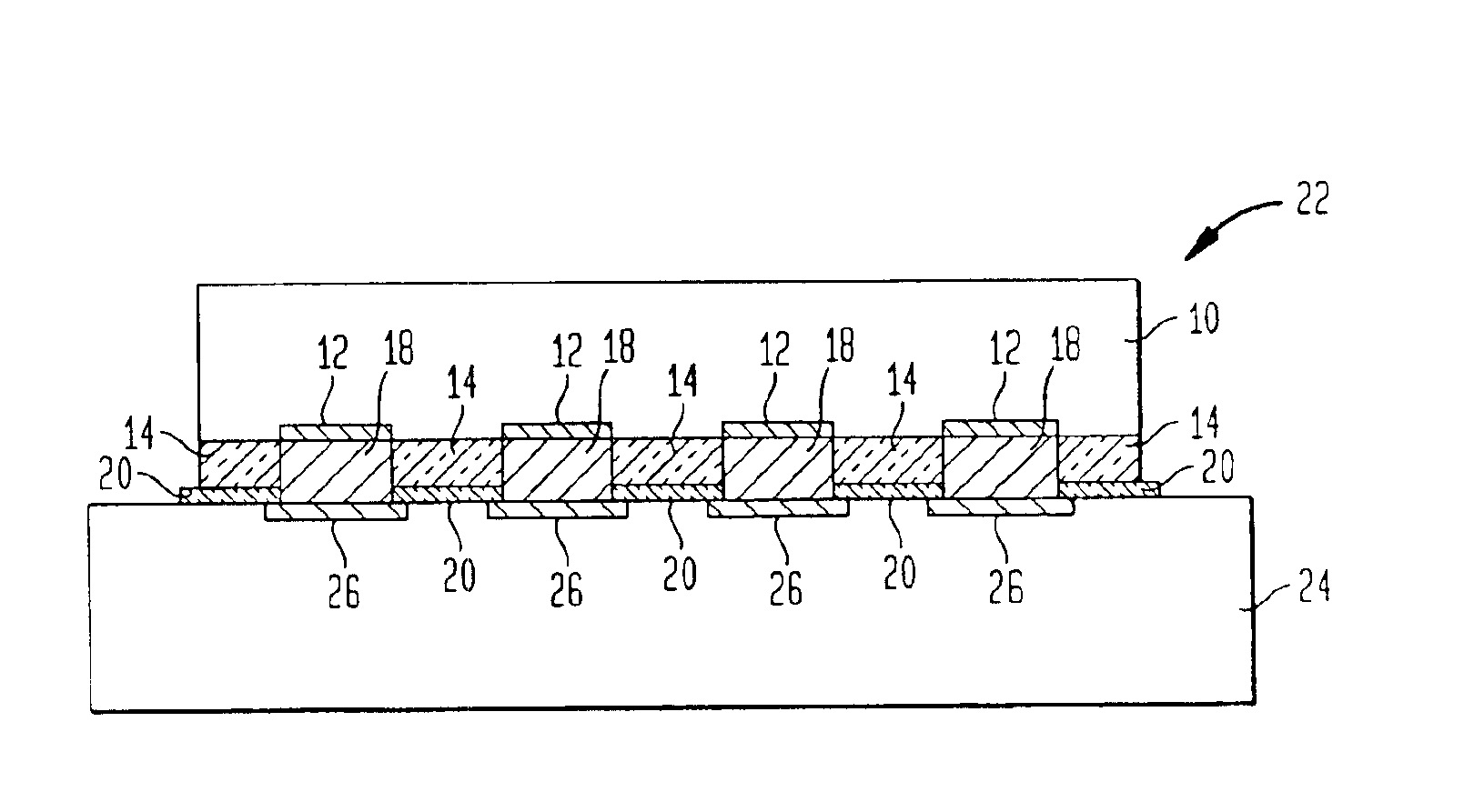
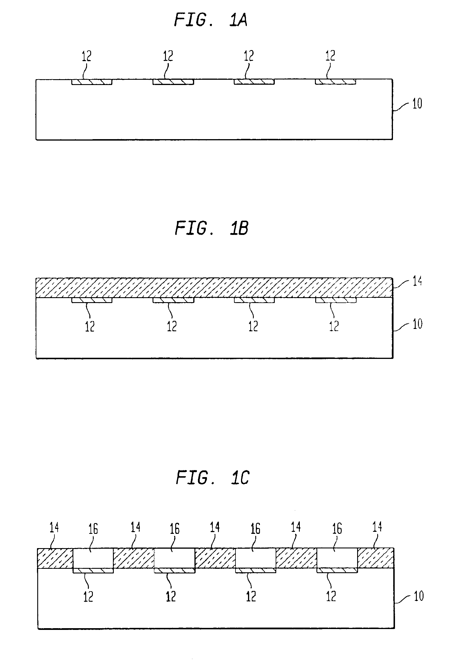
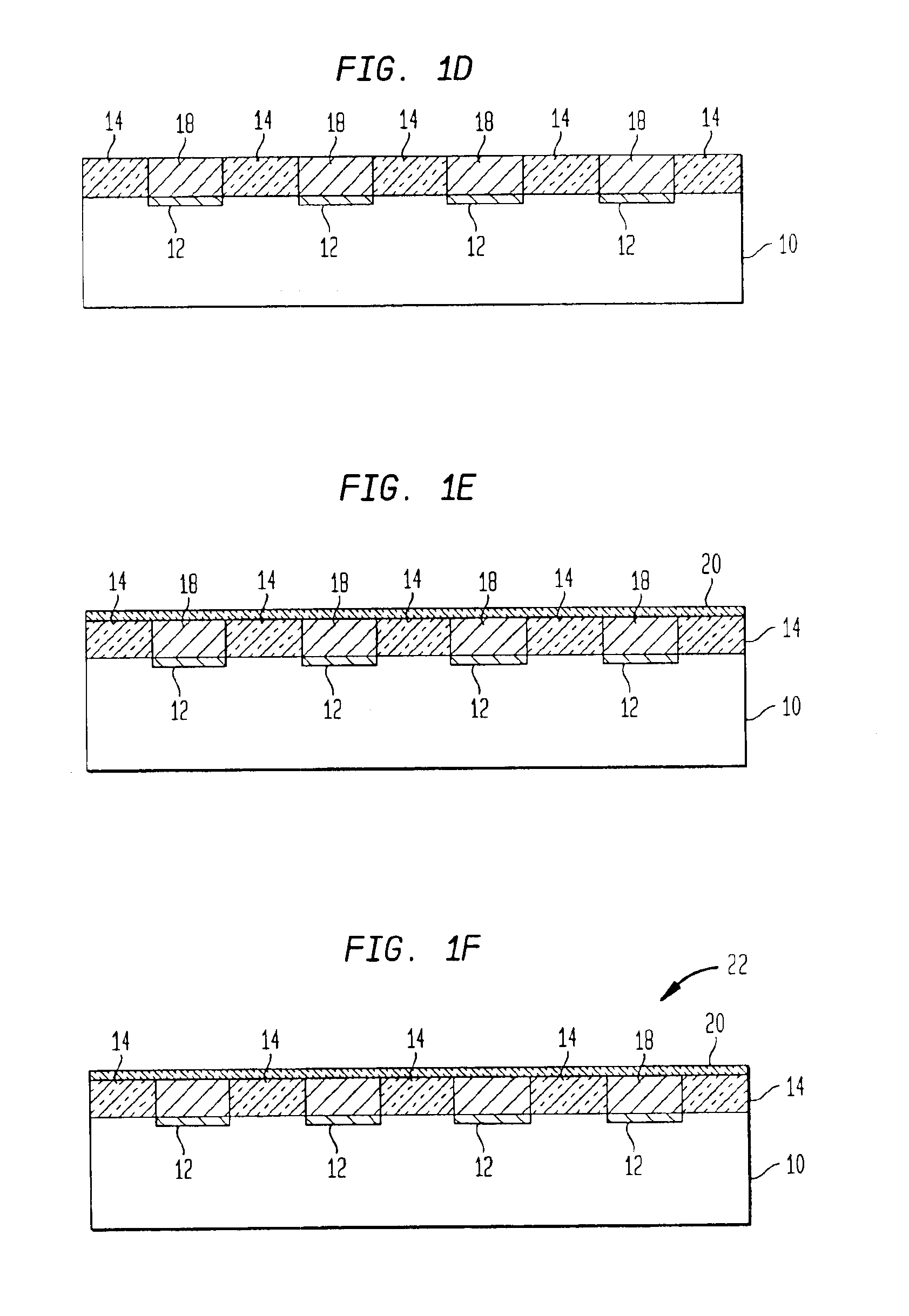
[0035]The present invention which provides a microelectronic interconnect structure and a method of fabricating the same will now be described in more detail by referring to the drawings that accompany the present application. It is noted that in these drawings, like and / or corresponding elements are referred to by like reference numerals.

[0036]Reference is first made to FIG. 1A which illustrates an initial structure that can be employed in the present invention. Specifically, the initial structure shown in FIG. 1A comprises semiconductor wafer 10 having interconnect pads 12 formed on predetermined portions of the wafer. The structure shown in FIG. 1A is comprised of conventional materials well known to those skilled in the art and conventional processing steps are used in fabricating the same.

[0037]For example, semiconductor wafer 10 is comprised of a semiconducting material including, but not limited to: Si, Ge, SiGe, GaAs, InAs, InP and all other II / V compound semiconductors. The...


PUM


Abstract

Methods for fabricating microelectronic interconnection structures as well as the structures formed by the methods are disclosed which improve the manufacturing throughput for assembling flip chip semiconductor devices. The use of a bilayer of polymeric materials applied on the wafer prior to dicing eliminates the need for dispensing and curing underfill for each semiconductor at the package level, thereby improving manufacturing throughput and reducing cost.

Description

[0001]This invention was made with Government support under Contract No. 1998-06-0030C awarded by NIST-ATP; therefore the Government has certain rights to the present invention.DESCRIPTION[0002]1. Field of the Invention[0003]The present invention relates to microelectronic packaging, and more particularly to a microelectronic interconnect structure and to a method of fabricating the same. The inventive method which utilizes a bilayer polymeric underfill eliminates separate underfill steps that are typically required in prior art methods of fabricating microelectronic interconnect structures.[0004]2. Background of the Invention[0005]Flip chip technology has grown rapidly in recent years as a means of decreasing the chip footprint while simultaneously increasing the number of possible I / O's. This is because flip chip technology takes advantage of the chip area for I / O's instead of just the chip periphery as does wire bonding. Various methods exist for solder bumping wafers, such as ev...

Claims


Application Information

Patent Timeline
Patent Type & Authority Patents(United States)
IPC IPC(8): H01L21/56H01L21/60H01L23/28H01L21/02H01L23/29
CPCH01L21/563H01L23/295H01L24/11H01L24/27H01L24/94H01L24/29H01L2224/1147H01L2224/13099H01L2224/16225H01L2224/274H01L2224/73203H01L2224/73204H01L2224/83191H01L2924/01005H01L2924/01022H01L2924/01029H01L2924/01032H01L2924/01047H01L2924/0105H01L2924/01078H01L2924/01082H01L2924/10329H01L2924/12044H01L2924/19041H01L2924/01006H01L2924/01023H01L2924/01033H01L2924/014H01L2924/0132H01L2924/0133H01L2924/01083H01L2224/2919H01L2924/0665H01L2224/29111H01L2224/13111H01L2924/00014H01L2924/10253H01L2924/00H01L2224/05571H01L2224/05573H01L2224/73104H01L2924/12042H01L2224/05599
Inventor BUCHWALTER, STEPHEN L.DANOVITCH, DAVIDDOANY, FUAD ELIASFEGER, CLAUDIUSGRUBER, PETER A.IYENGAR, REVATHILABIANCA, NANCY C.
Owner IBM CORP
Why Eureka
Try Eureka