Liquid crystal display device

a liquid crystal display and display device technology, applied in non-linear optics, instruments, optics, etc., can solve the problems of difficult to realize stable production of the device, narrow viewing angle of conventional twist nematic and super twist nematic liquid crystal display devices, and high risk of rubbing streaks in the displayed image, etc., to achieve the effect of suppressing voltage drop

Inactive Publication Date: 2005-08-02
SHARP KK
View PDF19 Cites 78 Cited by
  • Summary
  • Abstract
  • Description
  • Claims
  • Application Information

AI Technical Summary

Benefits of technology

[0014]The dielectric layer may include a depressed portion or an opening in the at least one first opening. With a structure where the dielectric layer includes a depressed portion or an opening, it is possible to suppress the voltage drop due to the dielectric layer. Moreover, it is possible

Problems solved by technology

However, conventional twist nematic (TN) type and super twist nematic (STN) type liquid crystal display devices have a narrow viewing angle.
While the transverse electric field mode is an effective approach to improve the viewing angle, the production process thereof imposes a significantly lower production margin than that of a normal TN type device, whereby it is difficult to realize stable production of the device.
However, when a vertical alignment film is subjected to a rubbing treatment, rubbing streaks are likely to appear in the displayed image, and it is not su

Method used


Image

  • Liquid crystal display device
  • Liquid crystal display device
  • Liquid crystal display device

Examples


embodiment 1

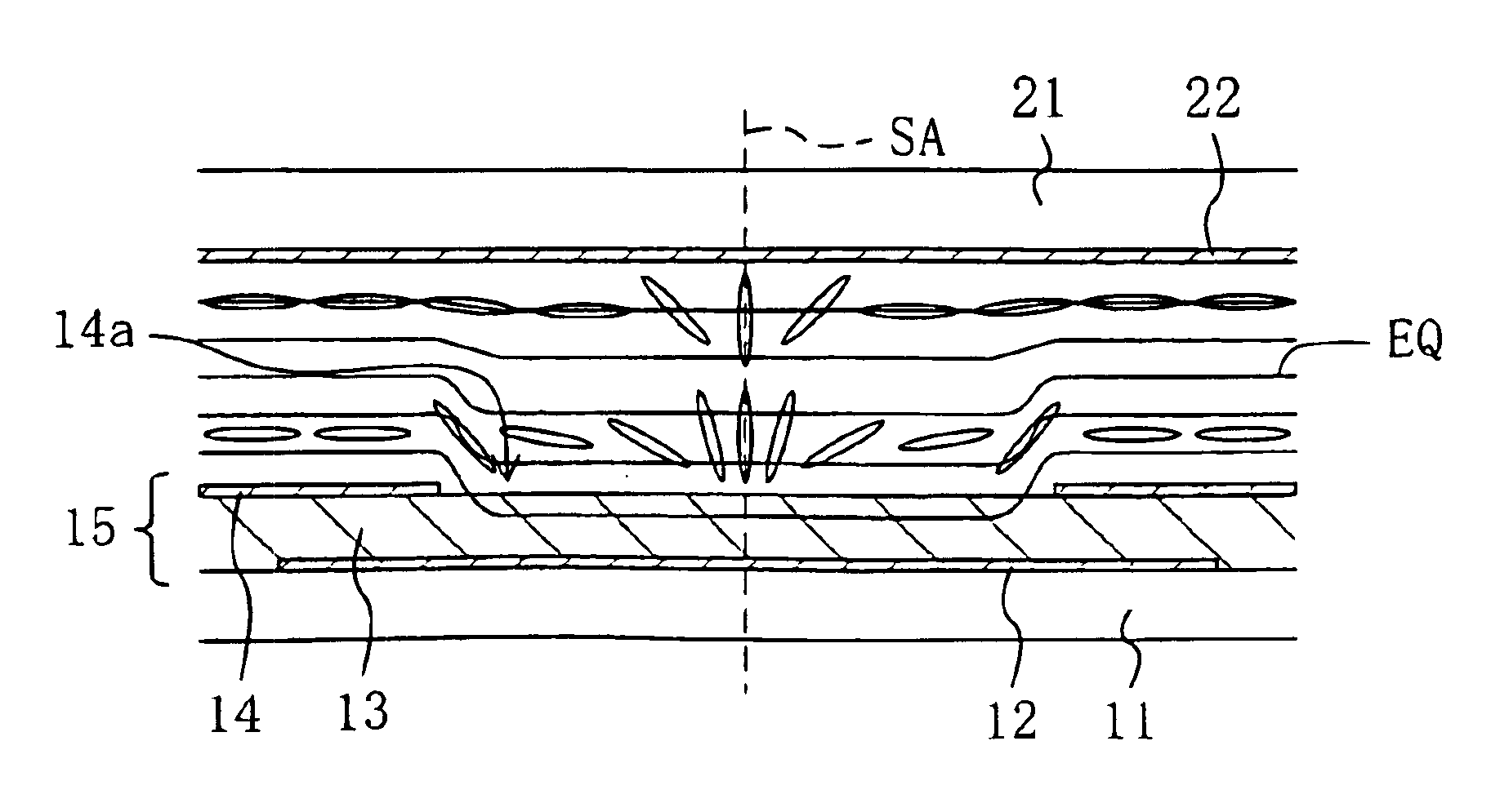
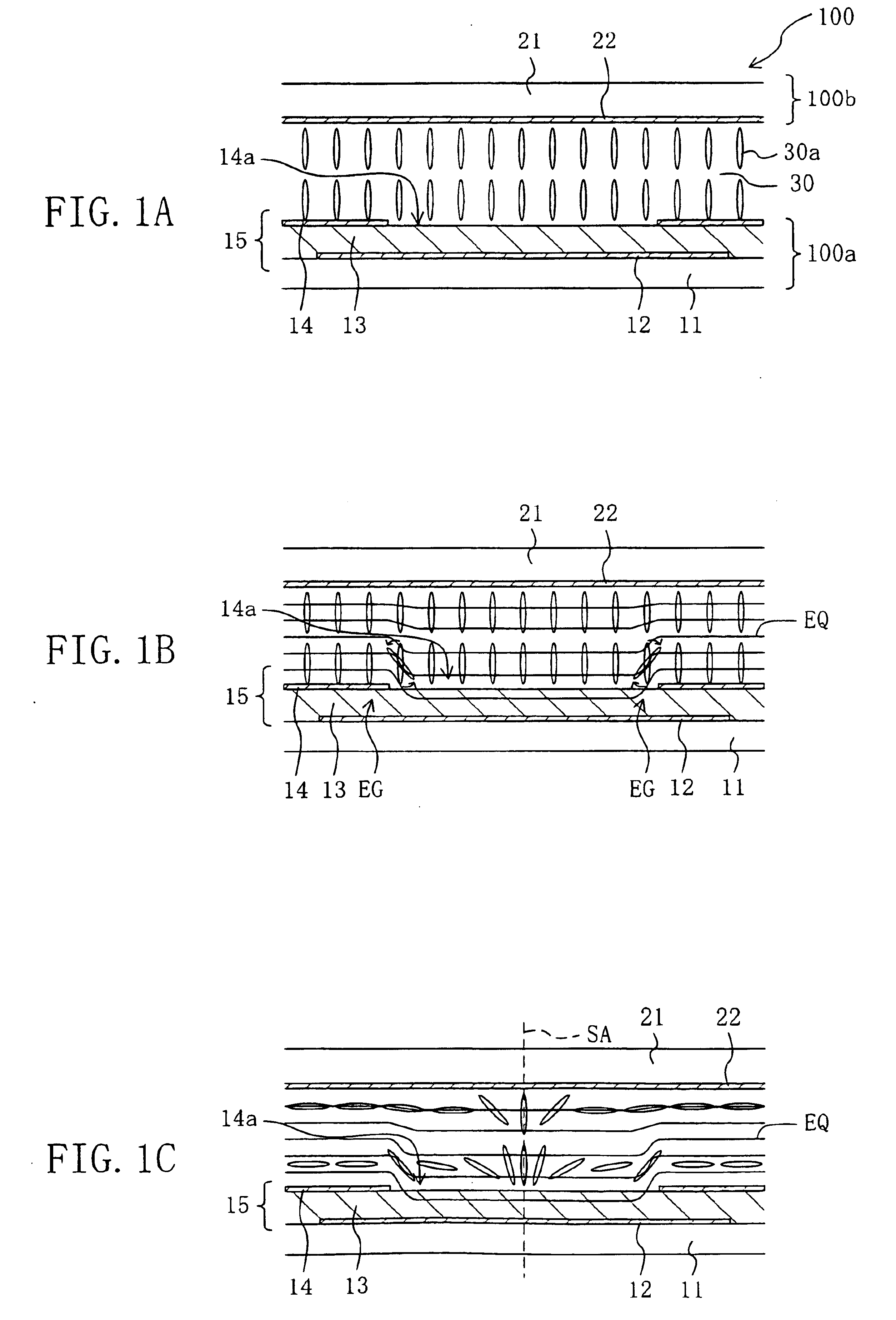
[0134]First, the electrode structure of the liquid crystal display device of the present invention and the function thereof will be described. The liquid crystal display device of the present invention has desirable display characteristics and is therefore suitably used as an active matrix type liquid crystal display device. While the preferred embodiments of the present invention will be hereinafter described with respect to an active matrix type liquid crystal display device using thin film transistors (TFTs), the present invention can alternatively be used with an active matrix type liquid crystal display device using an MIM (metal-insulator-metal) structure, or a passive matrix type liquid crystal display device. Moreover, while the preferred embodiments of the present invention will be described with respect to a transmission type liquid crystal display device, the present invention can alternatively be used with a reflection type liquid crystal display device or even with a tr...

embodiment 2

[0244]The structure of one picture element region of a liquid crystal display device 400B according to Embodiment 2 of the present invention will now be described with reference to FIG. 23A and FIG. 23B. In the subsequent figures, each element having substantially the same function as that of the liquid crystal display device 400 illustrated in FIG. 11A to FIG. 11c will be denoted by the same reference numeral and will not be further described. FIG. 23A is a plan view as viewed in the substrate normal direction, and FIG. 23B is a cross-sectional view taken along line 23B-23B′ of FIG. 23A. FIG. 23B schematically illustrates a state where no voltage is applied across the liquid crystal layer.

[0245]As illustrated in FIG. 23A and FIG. 23B, the liquid crystal display device 400B is different from the liquid crystal display device 400A of Embodiment 1 illustrated in FIG. 15A and FIG. 15B in that a TFT substrate 400b of the liquid crystal display device 400B includes a protrusion 40 in the...

embodiment 3

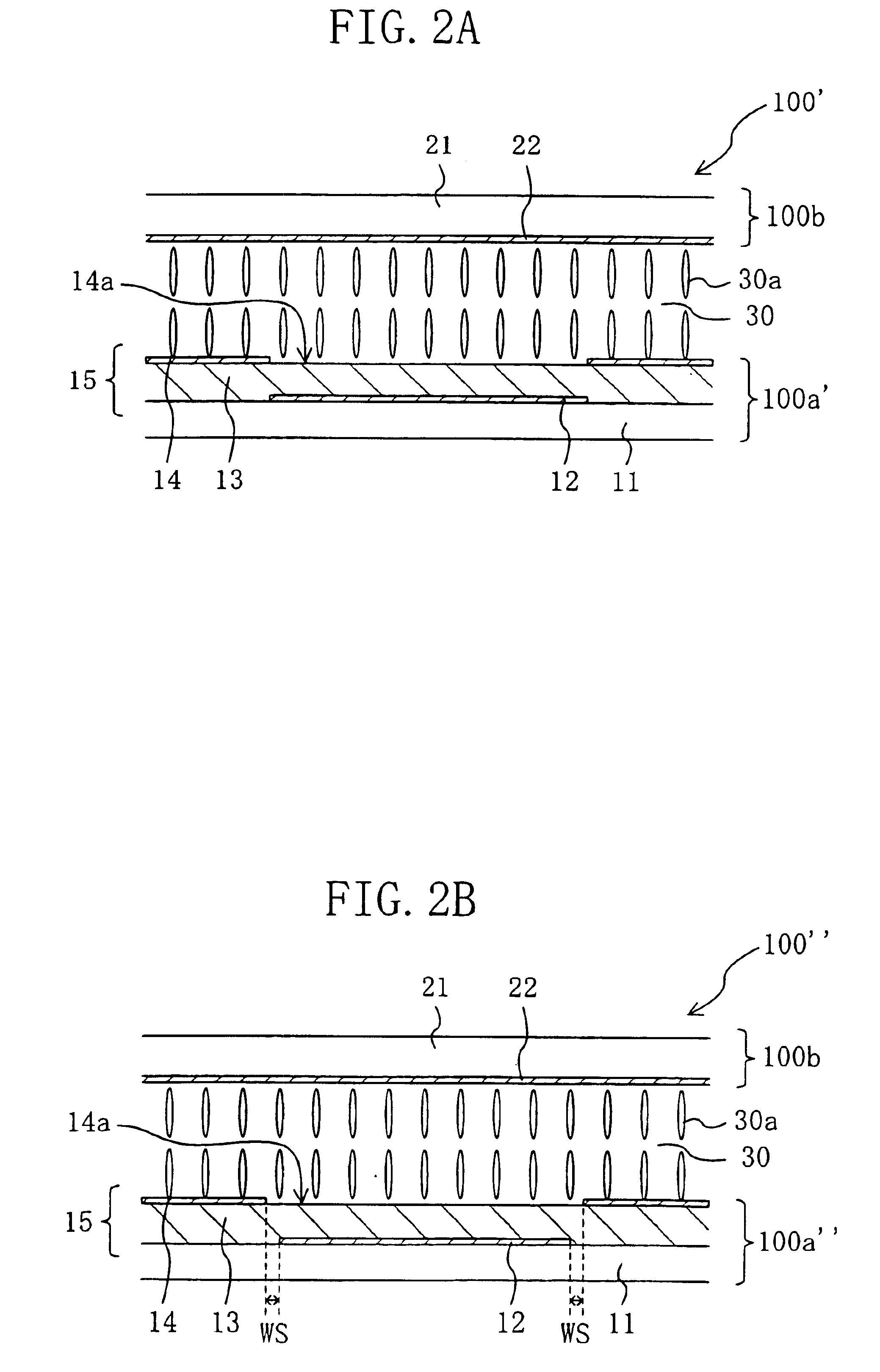
[0271]In the liquid crystal display device of Embodiment 1 described above, a two-layer electrode is employed for one (the picture element electrode 15 in the illustrated example) of the picture element electrode 15 defining picture element regions and the counter electrode 22 opposing each other via the liquid crystal layer 30, and the openings 14a are provided in the upper conductive layer 14, so that an inclined electric field is produced in the presence of an applied voltage, thereby orienting the liquid crystal molecules into a radially-inclined orientation by using the inclined electric field. In the liquid crystal display device of Embodiment 2, the protrusion is provided in the opening 14a of the upper conductive layer 14 so as to stabilize the radially-inclined orientation.

[0272]Embodiment 3 is a liquid crystal display device including a further orientation-regulating structure provided on the substrate (the counter substrate in the examples described above) which is differ...


PUM


Abstract

The present invention provides a liquid crystal display device having a high display quality. The liquid crystal display device displays an image by applying a voltage by a first electrode and a second electrode across a liquid crystal layer which takes a vertical alignment in the absence of an applied voltage. The first electrode includes a lower conductive layer, a dielectric layer covering at least a portion of the lower conductive layer, and an upper conductive layer provided on one side of the dielectric layer which is closer to the liquid crystal layer. The upper conductive layer includes a first opening, and the lower conductive layer is provided so as to oppose at least a portion of the first opening via the dielectric layer.

Description

BACKGROUND OF THE INVENTION[0001]The present invention relates to a liquid crystal display device. More specifically, the present invention relates to a liquid crystal display device having a wide viewing angle characteristic and capable of performing a high quality display.[0002]In recent years, liquid crystal display devices, which are thin and light in weight, are used for personal computers and PDA (personal digital assistance) devices. However, conventional twist nematic (TN) type and super twist nematic (STN) type liquid crystal display devices have a narrow viewing angle. Various technical developments have been undertaken to solve the problem.[0003]A typical technique for improving the viewing angle characteristic of a TN or STN type liquid crystal display device is to add an optical compensation plate thereto. Another approach is to employ a transverse electric field mode in which a horizontal electric field with respect to the substrate plane is applied across the liquid c...

Claims


Application Information

Patent Timeline
IPC IPC(8): G02F1/13G02F1/1333G02F1/1343G02F1/139G02F1/1337
CPCG02F1/133707G02F1/134336G02F1/133555G02F1/1393G02F1/1337
Inventor KUBO, MASUMIYAMAMOTO, AKIHIROOCHI, TAKASHIMAEKAWA, KAZUHIROFUJIOKA, SHOHGO
Owner SHARP KK
Why Eureka
Try Eureka