Optical waveguide circuit
- Summary
- Abstract
- Description
- Claims
- Application Information
AI Technical Summary
Benefits of technology
Problems solved by technology
Method used
Image
Examples
embodiment 1
[Embodiment 1]
[0048]FIGS. 4, 5A and 5B are views showing the first embodiment of the optical waveguide circuit in accordance with the present invention: FIG. 4 is a plan view of the optical waveguide circuit; FIG. 5A is a cross-sectional view taken along the line VA-VA′ in FIG. 4; and FIG. 5B is a cross-sectional view taken along the line VB-VB′ in FIG. 4. In these figures, the reference numeral 21 designates a Si substrate, and 28 designates a cladding. The reference numerals 22-27 each designate a shape of a waveguide core. The reference numeral 22 designates an input terminal section, 23 designates a tapered section, 24 designates an intersecting section, 25 designates a tapered section, and 26 designates an output terminal section. The reference numerals 27 each designate a waveguide intersecting with the intersecting section 24.
[0049]Assume that the waveguide core has a width w1 at the input terminal section 22 and output terminal section 26, and w2 at the intersecting section ...
embodiment 2
[Embodiment 2]
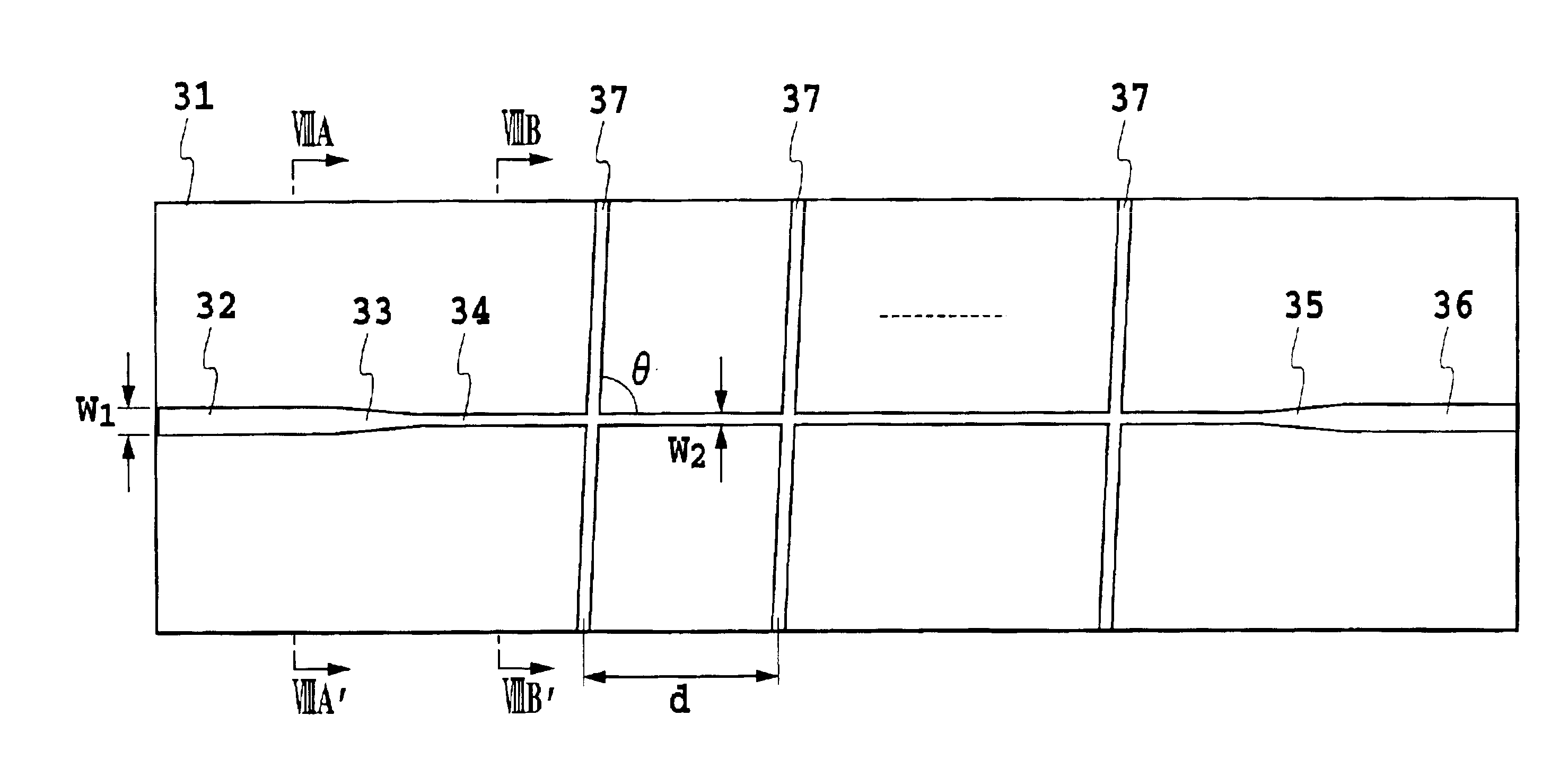
[0053]FIGS. 7, 8A and 8B are views showing the second embodiment of the optical waveguide circuit in accordance with the present invention: FIG. 7 is a plan view of the optical waveguide circuit; FIG. 8A is a cross-sectional view taken along the line VIIIA-VIIIA′ in FIG. 7; and FIG. 8B is a cross-sectional view taken along the line VIIIB-VIIIB′ in FIG. 7. In these figures, the reference numeral 31 designates a Si substrate, and 38 designates a cladding. The reference numerals 32-37 each designate a shape of a waveguide core. The reference numeral 32 designates an input terminal section, 33 designates a tapered section, 34 designates an intersecting section, 35 designates a tapered section, and 36 designates an output terminal section. The reference numerals 37 each designate a waveguide intersecting with the intersecting section 34.
[0054]Assume that the waveguide core has a width w1 at the input terminal section 32 and output terminal section 36, and w2 at the intersec...
embodiment 3
[Embodiment 3]
[0058]FIG. 10 is a plan view showing a third embodiment of the optical waveguide circuit in accordance with the present invention, in which the optical waveguide circuit in accordance with the present invention is applied to an N×N wavelength optical multi / demultiplexer. In FIG. 10, the reference numeral 41 designates a Si substrate, and 42 designates an N×2N AWG with N input waveguides and 2N output waveguides. The N input waveguides constitute the input ports of the N×N wavelength optical multi / demultiplexer. Reference numerals 43-47 designate one of 2N connecting waveguides including intersections. The reference numeral 43 designates an input terminal section, 44 designates an tapered section, 45 designates an intersecting section, 46 designates an tapered section, and 47 designates an output terminal section. Reference numerals 48 each designate one of N optical couplers for coupling two optical inputs. Each optical coupler consists of a multi-mode interferometer i...
PUM
 Abstract
Description
Claims
Application Information


