Methods for making semiconductor device structures with capacitor containers and contact apertures having increased aspect ratios

a technology of capacitor container and contact aperture, which is applied in the direction of capacitors, semiconductor devices, electrical equipment, etc., can solve the problems of limited use of capacitor containers, limited surface area of capacitor containers, and limited usefulness of capacitor containers, so as to achieve the effect of increasing the aspect ratio

Inactive Publication Date: 2005-08-09
MICRON TECH INC
View PDF17 Cites 26 Cited by
  • Summary
  • Abstract
  • Description
  • Claims
  • Application Information

AI Technical Summary

Benefits of technology

[0016]The present invention further includes semiconductor device structures and methods of making such structures that include one or more capacitor containers, contact apertures, or other openings therein having increased aspect ratios. The semiconductor device structures are formed by stacking an interlayer or cover layer atop a first structural layer and, subsequently, stacking a second structural layer atop the cover layer. Stepwise etching of capacitor containers, contact apertures, or other openings in the first and second structural layers and the cover layer provides increased height-to-width ratios of the resultant capacitor containers, contact apertures, or other openings.
[0018]Additionally, the present invention includes a method for self-aligning openings in substantially vertically stacked structural layers of a semiconductor device structure. Etching of the structural layers, generally in a stepwise fashion, may result in semiconductor device structures having openings therein with increased aspect ratios.

Problems solved by technology

However, DRAM capacitors of sufficient size to store and maintain the requisite amount of charge to permit the necessary refresh time must still be provided.
However, a change in material would cause a substantial interference with existing semiconductor manufacturing processes and, thus, such solution is undesirable.
While this technique creates a capacitor container with an increased surface area relative to a similarly sized capacitor container that is not lined with HSG polysilicon, surface area is still limited by the confines of the capacitor container structure.
However, the usefulness of this technique is similarly limited by the confines of the capacitor container in that a particular geometrical layout in a capacitor container having a smaller width will have a lesser surface area than a similar geometrical layout in a capacitor container having a larger width and a substantially equivalent height.
However, there are limitations to forming a large height-to-width ratio using known etching techniques due to the limitations of selective etching.
For instance, preservation of the surface underlying the etched layer may become compromised if the aspect ratio of the capacitor container is too great.
However, as contact apertures typically are etched, formation of a large height-to-width ratio is limited by the limitations of selective etching, as previously described.

Method used


Image

  • Methods for making semiconductor device structures with capacitor containers and contact apertures having increased aspect ratios
  • Methods for making semiconductor device structures with capacitor containers and contact apertures having increased aspect ratios
  • Methods for making semiconductor device structures with capacitor containers and contact apertures having increased aspect ratios

Examples


Embodiment Construction

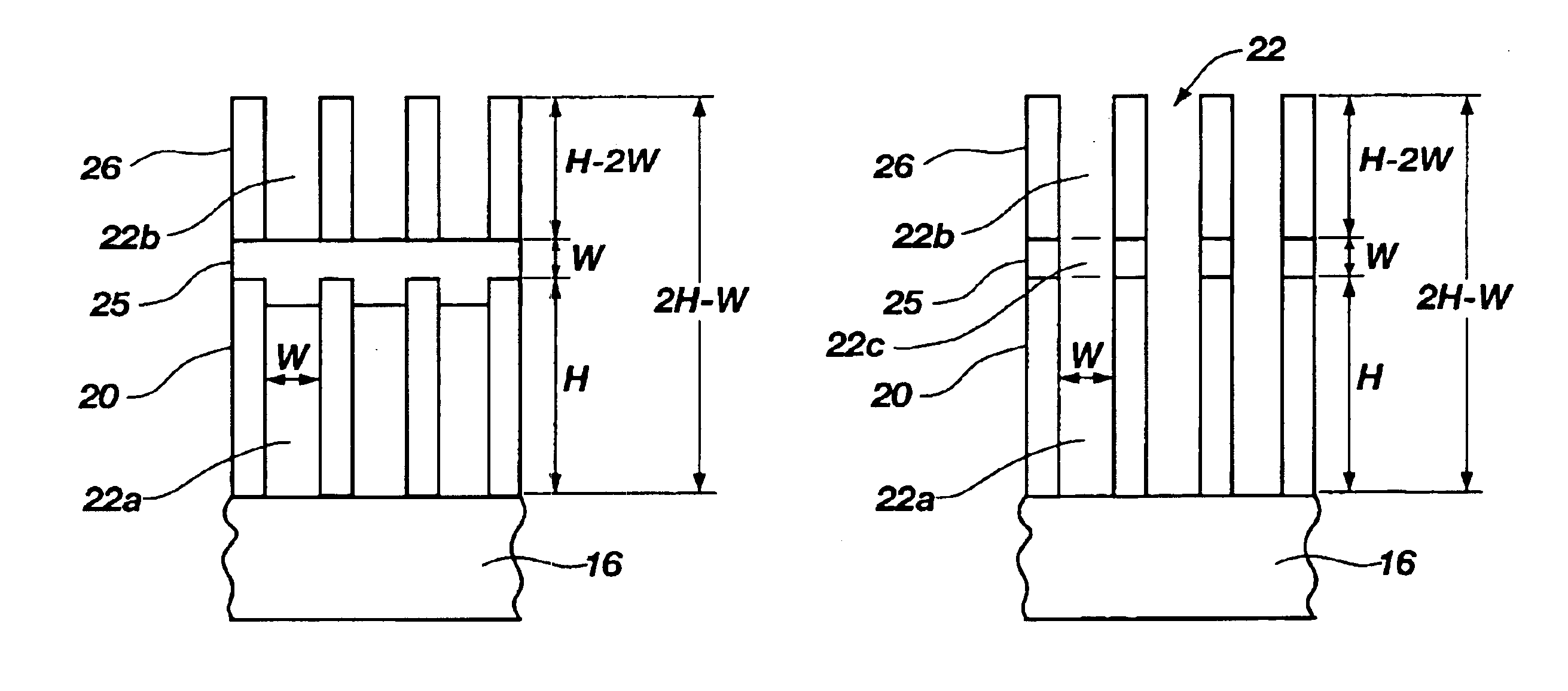
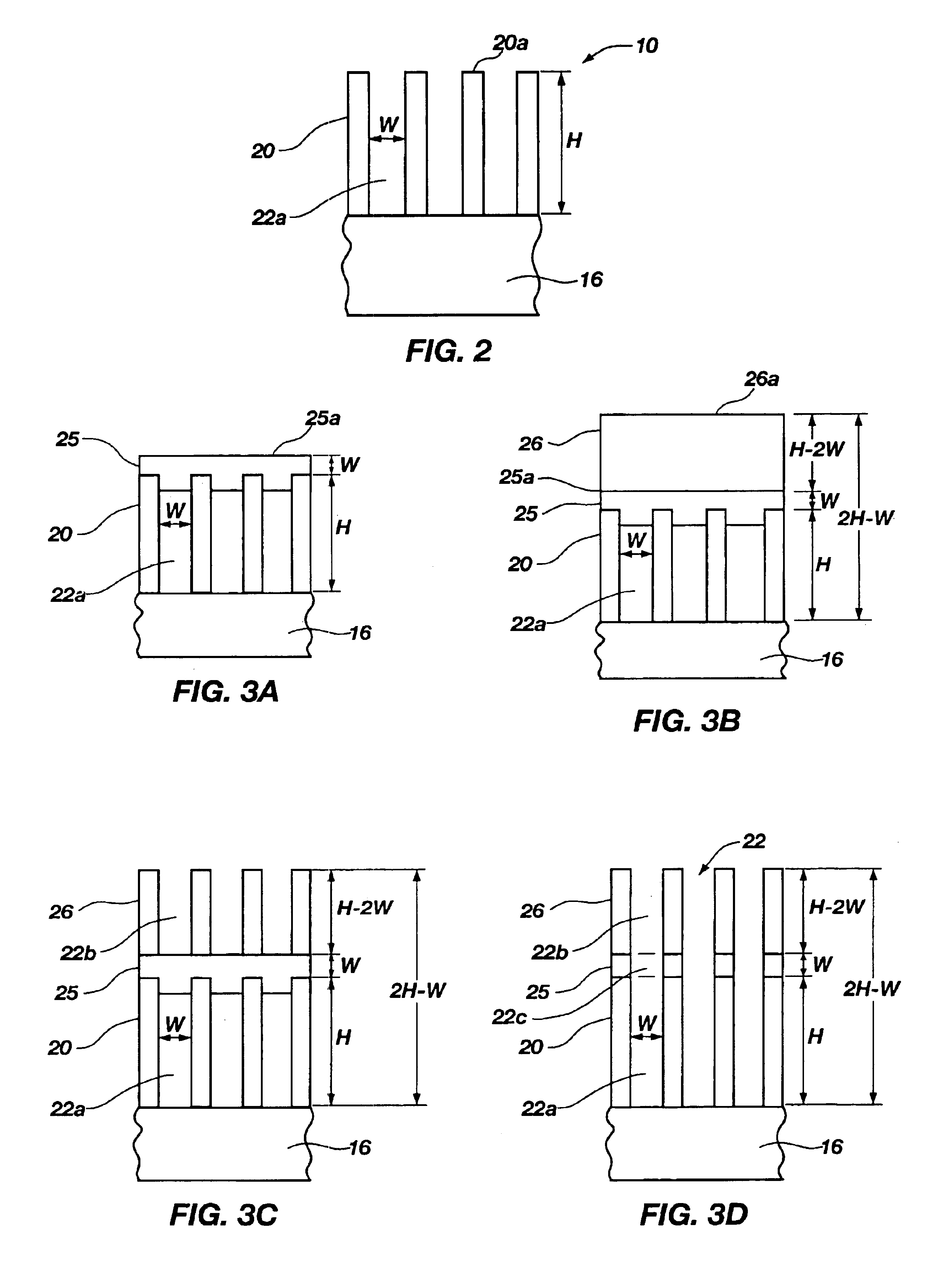
[0033]The present invention is directed to semiconductor device structures and methods of making such structures that include one or more capacitor containers, contact apertures, or other openings therein with increased height-to-width ratios. The particular embodiments described herein are intended in all respects to be illustrative rather than restrictive. Alternative embodiments will become apparent to those of ordinary skill in the art to which the present invention pertains without departing from its scope.

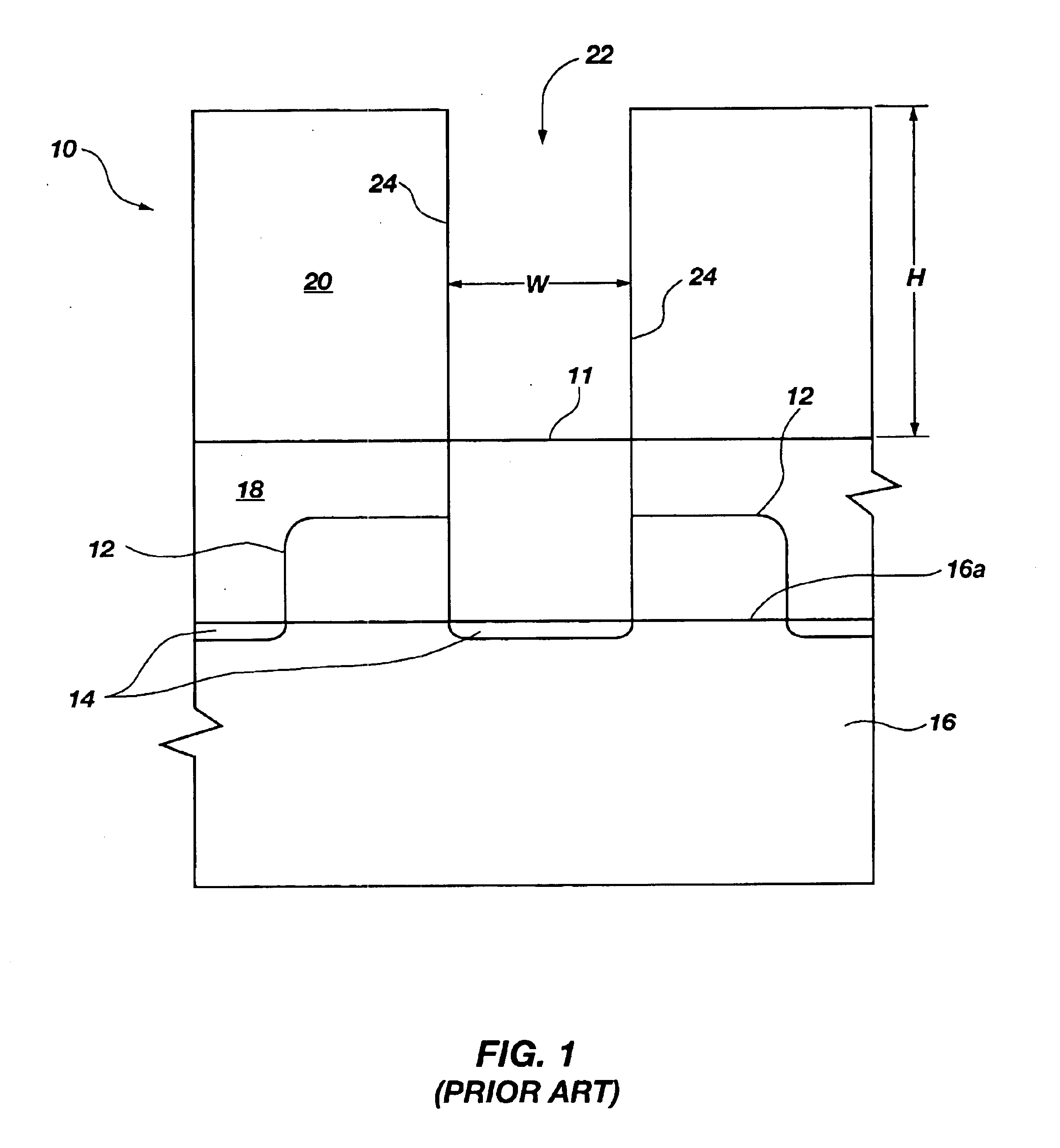
[0034]Referring initially to FIG. 2, an exemplary semiconductor device structure 10 is shown. The semiconductor device structure of FIG. 2 includes a plurality of capacitor container portions 22a formed in a first structural layer 20, such as a phosphosilicate glass (PSG) layer, a borosilicate glass (BSG) layer, or a borophosphosilicate glass (BPSG) layer. Conventional techniques for forming a semiconductor device structure as depicted in FIG. 2 are known in the art and will ...


PUM


Abstract

Semiconductor device structures and methods of making such structures that include one or more etched openings (e.g., capacitor containers and / or contact apertures) therein with increased height-to-width ratios are provided. The structures of the present invention are formed by successive layer deposition wherein conventional patterning techniques may be utilized in a stepwise fashion as the height of the structure is increased. Further provided is a self-aligning interconnection structure which may be used to substantially vertically align openings formed in successively deposited, vertically placed structural layers of a semiconductor device. The interconnection structure utilizes a cap-and-funnel model that self-aligns to the center plane of an opening in a first structural layer and also substantially prevents subsequently deposited material from entering the opening.

Description

CROSS-REFERENCE TO RELATED APPLICATION[0001]This application is a continuation of application Ser. No. 10 / 329,913, filed Dec. 26, 2002, now U.S. Pat. No. 6,812,150, issued Nov. 2, 2004.BACKGROUND OF THE INVENTION[0002]1. Field of the Invention[0003]The present invention relates generally to the fabrication of semiconductor device structures. More particularly, the present invention relates to semiconductor device structures with capacitor containers, contact apertures, or other openings therein that have increased height-to-width ratios. Further, the present invention relates to methods of making semiconductor device structures having capacitor containers, contact apertures, or other openings therein with increased aspect ratios.[0004]2. Background of the Related Art[0005]In computer semiconductor devices, such as dynamic random access memory (DRAM) semiconductor device modules, the memory capacitors typically are formed inside containers, such as phosphosilicate glass (PSG), borosi...

Claims


Application Information

Patent Timeline
Patent Type & Authority Patents(United States)
IPC IPC(8): H01L21/02H01L21/60H01L21/768H01L21/8242H01L27/108
CPCH01L21/76802H01L21/76897H01L27/10811H01L27/10817H01L27/10852H01L27/10888H01L28/91H01L28/84H10B12/312H10B12/318H10B12/033H10B12/485
Inventor ZHENG, LINGYI A.
Owner MICRON TECH INC
Why Eureka
Try Eureka