Method of manufacturing electron source and image display apparatus

a technology of electron source and image display, which is applied in the manufacture of electrode systems, tube/lamp factory adjustment, and screen, etc., can solve the problems of large voltage drop, device cannot receive a sufficient voltage, and does not exactly show the actual position and shape of the electron-emitting portion, so as to reduce the power source capacity of the apparatus, reduce the reactive current, and avoid any luminance variation

Inactive Publication Date: 2005-08-16
CANON KK
View PDF5 Cites 5 Cited by
  • Summary
  • Abstract
  • Description
  • Claims
  • Application Information

AI Technical Summary

Benefits of technology

[0029]It is another object of the present invention to provide a method of manufacturing an image display apparatus almost free from any luminance variations.
[0030]It is still another object of the present invention to reduce a reactive current in the electrification step in manufacturing an electron source having a plurality of electron-emitting devices and an image display apparatus using the electron source.
[0031]It is still another object of the present invention to reduce the power source capacity of an apparatus used in the electrification step in manufacturing an electron source having a plurality of electron-emitting devices and an image display apparatus using the electron source.
[0032]It is still another object of the present invention to provide a method of manufacturing an electron source which prevents deterioration of electron-emitting devices in manufacture and driving, and manufacturing an image display apparatus using the electron source.

Problems solved by technology

However, this does not exactly show the actual position and shape of the electron-emitting portion.
However, the activation processing applied to multi surface-conduction type emission devices arranged in a simple matrix poses the following problems.
Problems occur when devices arranged in a large matrix are activated in units of rows.
Some devices cannot receive a sufficient voltage, which varies the electron-emitting characteristics of respective devices.
However, a larger matrix size causes a larger voltage drop under the influence of the wiring resistance of a row wiring, so no predetermined voltage can be applied.
In particular, a desired voltage cannot be applied to devices at almost the center of the row wiring.
These devices cannot be satisfactorily activated, thus varying the characteristics of devices arranged in a matrix.

Method used


Image

  • Method of manufacturing electron source and image display apparatus
  • Method of manufacturing electron source and image display apparatus
  • Method of manufacturing electron source and image display apparatus

Examples


first embodiment

[0083]In the first embodiment, surface-conduction type emission devices are arranged in a matrix. The low-resistance phenomenon of unselected devices that occurs in activating devices while compensating for a voltage drop caused by the wiring resistance is detected on the whole matrix. When the low-resistance phenomenon of devices is observed, a resistance increase pulse is applied to all devices to activate them.

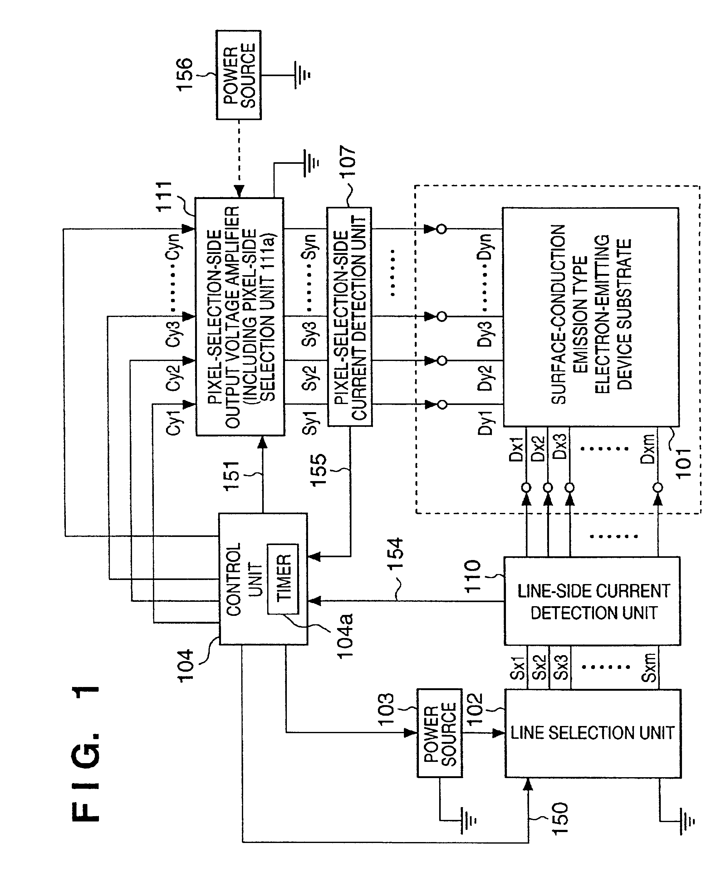
[0084]FIG. 1 is a block diagram showing an example of an activation apparatus for surface-conduction type emission devices according to the first embodiment.

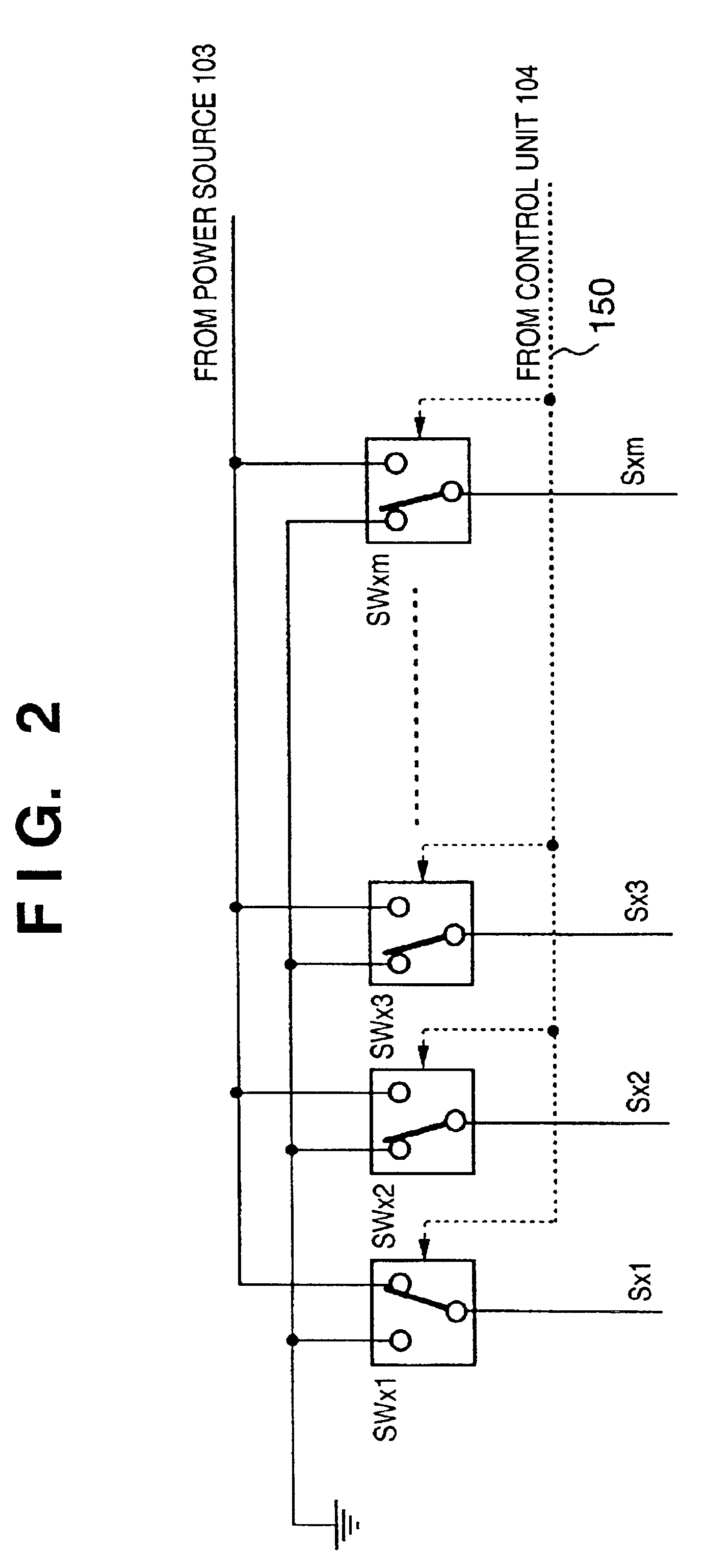
[0085]In FIG. 1, reference numeral 101 denotes a multi surface-conduction type emission device (electron source)substrate (on the substrate 101 of the first embodiment, a plurality of surface-conduction type emission devices are arranged in a matrix and have already undergone forming processing). The substrate 101 is connected to an evacuation device (not shown). A vessel storing this substrate 101 is evacuated to about...

second embodiment

[0131]The second embodiment detects, in units of column wirings, the low-resistance phenomenon of unselected devices that occurs in activating devices while compensating for a voltage drop caused by wiring surface-conduction type emission devices in a matrix. When the low-resistance phenomenon of devices is detected, a resistance increase pulse is applied in units of column wirings to activate the devices.

[0132]The second embodiment according to the present invention will be described in detail.

[0133]An activation apparatus in the second embodiment has the same arrangement as in the first embodiment, and a surface-conduction type emission device is also identical to that in the first embodiment. Thus, a description of the whole apparatus arrangement will be omitted.

[0134]The second embodiment is different from the first embodiment in a method of detecting a low-resistance device among surface-conduction type emission devices and a method of applying a resistance increase pulse. In t...

third embodiment

[0150]The third embodiment detects, in units of devices, the low-resistance phenomenon of unselected devices that occurs in activating devices while compensating for a voltage drop caused by wiring surface-conduction type emission devices in a matrix. When the low-resistance phenomenon of devices is detected in units of devices, a resistance increase pulse is applied in units of devices to activate them.

[0151]The third embodiment according to the present invention will be described in detail.

[0152]An activation apparatus in the third embodiment has the same arrangement as in the first embodiment, and a surface-conduction type emission device substrate is also identical to that in the first embodiment. Thus, a description of the whole apparatus arrangement will be omitted.

[0153]The third embodiment is different from the first embodiment in a method of detecting a low-resistance device among surface-conduction type emission devices and a method of applying a resistance increase pulse....


PUM


Abstract

In a method of manufacturing an electron source, a plurality of row wirings, a plurality of column wirings, and a plurality of pairs of conductive films arranged in a matrix by the plurality of row and column wirings, are formed on a substrate, each pair of conductive films being formed through a gap. After then, a row wiring is selected among the plurality of row wirings in the presence of an activation substance source, and a substantially same constant voltage is applied to each of a plurality of pairs of conductive films connected to the selected row wiring, while a predetermined voltage is applied to at least specific pairs of conductive films among a plurality of pairs of conductive films connected to unselected row wirings of the plurality of row wirings.

Description

BACKGROUND OF THE INVENTION[0001]1. Field of the Invention[0002]The present invention relates to a method of manufacturing an electron source having an array of a plurality of electron-emitting devices, and manufacturing an image display apparatus using the electron source.[0003]2. Description of the Related Art[0004]Conventionally, two types of devices, namely hot and cold cathode devices, are known as electron-emitting devices. Known examples of the cold cathode devices are surface-conduction type emission devices, field emission type electron-emitting devices(to be referred to as FE type electron-emitting devices hereinafter), and metal / insulator / metal type electron-emitting devices (to be referred to as MIM type electron-emitting devices hereinafter).[0005]Known examples of the FE type electron-emitting devices are described in W. P. Dyke and W. W. Dolan, “Field emission”, Advance in Electron Physics, 8, 89 (1956) and C. A. Spindt, “Physical properties of thin-film field emissio...

Claims


Application Information

Patent Timeline
Patent Type & Authority Patents(United States)
IPC IPC(8): H01J9/00H01J9/44H01J9/02H01J31/12
CPCH01J9/027H01J31/127H01J2201/3165
Inventor TAKEGAMI, TSUYOSHI
Owner CANON KK
Why Eureka
Try Eureka