Liquid crystal device

Inactive Publication Date: 2005-08-16
SHARP KK
View PDF8 Cites 31 Cited by
  • Summary
  • Abstract
  • Description
  • Claims
  • Application Information

AI Technical Summary

Benefits of technology

[0031]It is an object of the invention to provide a liquid crystal display whose res

Problems solved by technology

However, TN-type TFT LCDs have a serious problem in that their viewing angles are small.
This is the most serious problem of TN-type LCDs.
Specifically, although they can achieve a high speed response when display is turned to black again after a change from black display to white display, they are somewhat inferior to TN-type TFT LCDs in terms of response time during a change from a certain halftone to another halftone.
Further, conventional MVA type TFT LCDs have optical transmittance which is about twice that of lateral field type IPS (In-plane switching) wide viewing angle LCDs but is not as good as that of TN-type TFT LCDs.
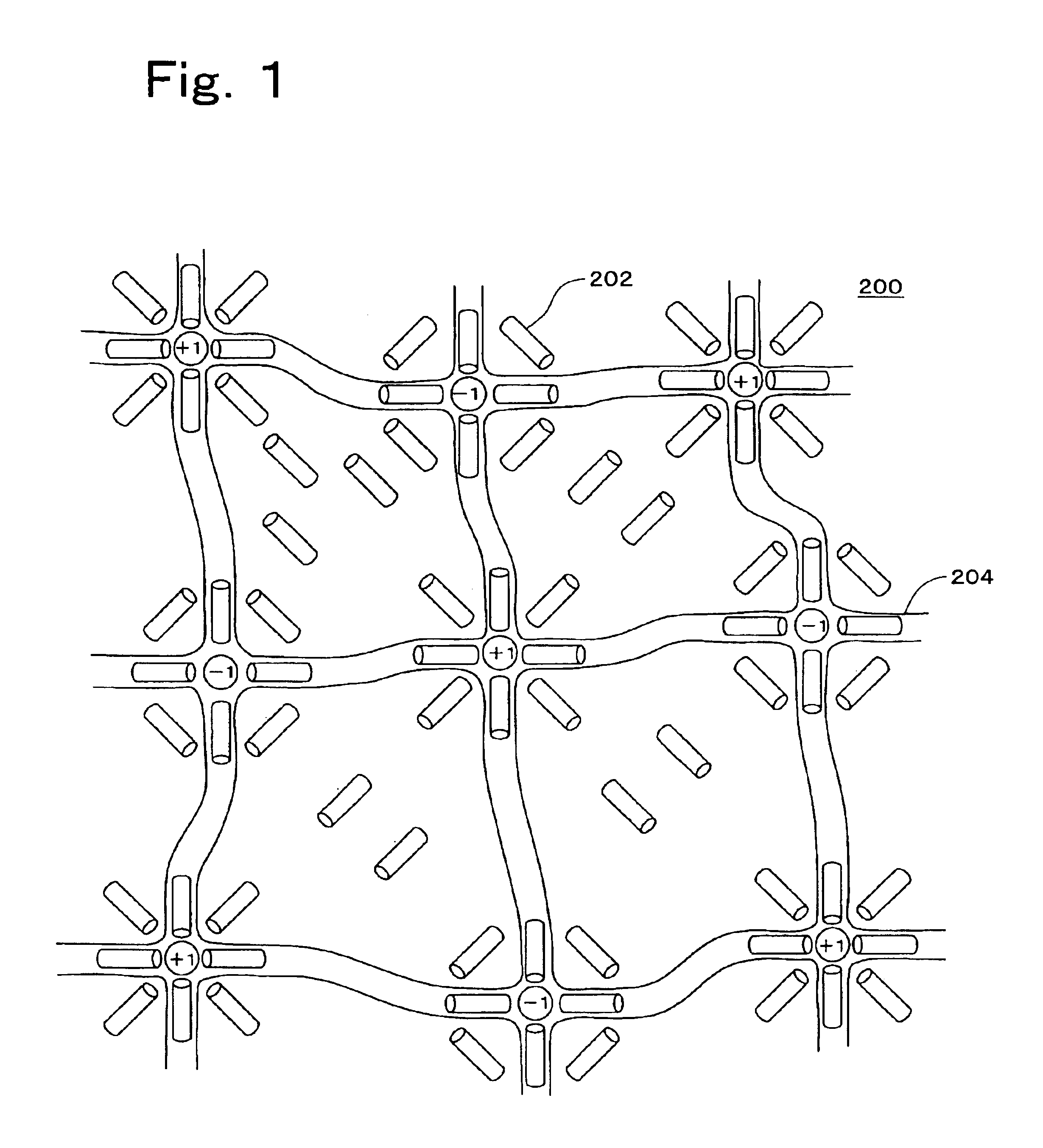
As described above, while MVA TFT LCDs have solved the problems with conventional LCDs in terms of the viewing angle, contrast and response time in displaying black, white and then black again, they are not still as good as conventional TN-type LCDs in term

Method used


Image

  • Liquid crystal device
  • Liquid crystal device
  • Liquid crystal device

Examples


embodiment 1

[Embodiment 1]

[0157]FIG. 36 shows Embodiment 1 in the present mode for carrying out the invention. A singular point forming portion in the present embodiment has regions formed by locally changing the width of bus lines 152 and 154. As shown in FIG. 36, a narrow region 60 and a wide region 62 are formed adjacent to each other with a region having a normal width interposed therebetween. While the normal width of the bus lines is 10 μm, the narrow region 60 and wide region 62 are 5 μm and 15 μm, respectively. The lengths of the narrow region 60 and wide region 62 in the extending direction of the bus lines 152 and 154 are both 10 μm.

[0158]A vertical alignment film 2 is applied to a lower substrate 118 on which the bus lines 152 and 154 formed with such narrow region 60 and wide region 62 of the singular point forming portion. The lower substrate is combined with an upper substrate 116 having a vertical alignment film 4 similarly applied thereto. Then, liquid crystals are injected. As ...

embodiment 2

[Embodiment 2]

[0160]Embodiment 2 will now be described with reference to FIGS. 37A through 37E. FIG. 37A shows a state of the bus lines 152 and 154 as viewed in the direction of the normal line of the substrate surface. FIG. 37B shows an example of a section taken along line A—A in FIG. 37A, and FIG. 37C shows another example of the same. FIG. 37D shows an example of a section taken along line B—B in FIG. 37A, and FIG. 37E shows another example of the same.

[0161]The present embodiment is characterized in that there is provided structures or blank regions on the bus lines 152 and 154 or on the opposite substrate directly above the bus lines 152 and 154 instead of the singular point forming portion described in Embodiment 1 in which the width of the bus lines is varied. The bus line width is 10 μm. In FIG. 37B, protruding structures 64 are formed on the bus lines 152 and 154 to form and fix second singular points. The width and length of the protruding structures 64 are both 5 μm, and...

embodiment 3

[Embodiment 3]

[0166]Embodiment 3 will now be described with reference to FIG. 38. A singular point forming portion in the present embodiment is configured by arranging a narrow region 60 formed by reducing the width of bus lines 152 and 154 and a non-electrode region 126 in the form of a slit formed at an edge 160 of a pixel electrode 122 as shown in FIG. 30 and so on such that they are adjacent to each other as viewed in the direction of the normal line of the substrate surface. While the bus line width is normally 10 μm, the width of the narrow region 60 is 5 μm, and the length of the narrow region 60 in the extending direction of the bus lines 152 and 154 is 10 μm.

[0167]Second singular points are formed on the bus lines 152 and 154 similarly to Embodiment 1, and first singular points are formed in the regions between the bus lines 152 and 154 and the edges 160 of the pixel electrodes 122. Like Embodiments 1 and 2, this also makes it possible to eliminate phenomena that are relate...


PUM


Abstract

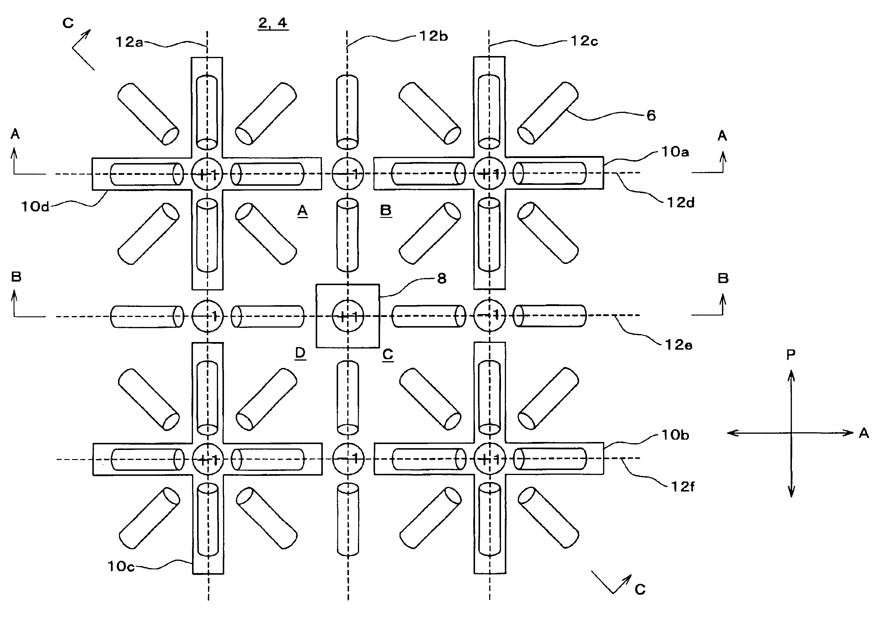
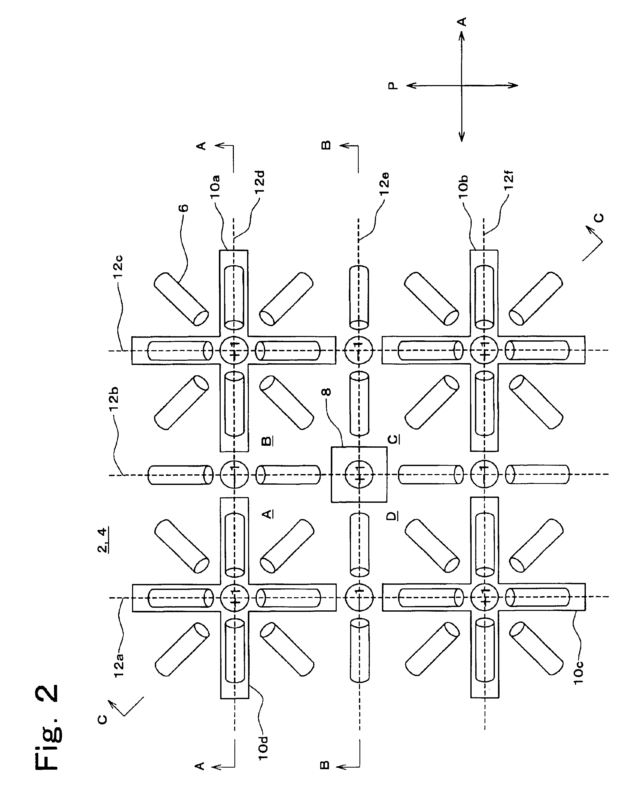
The present invention relates to a liquid crystal display in multiple alignment or MVA mode in which liquid crystal molecules having negative dielectric anisotropy are aligned differently, and it is an object of the invention to provide a liquid crystal display having improved response characteristics while suppressing any reduction in transmittance. In a liquid crystal display having an electrode formed on each of opposite surfaces of two substrates facing each other with a predetermined gap therebetween, vertical alignment films 2 and 4 formed on the electrodes and liquid crystal molecules 6 having negative dielectric anisotropy sealed between the two substrates, there is provided singular point control portions 10a through 10d and 8 for controlling singular points (+1 or −1) of an alignment vector field of the liquid crystal molecules 6 such that they are formed in predetermined positions when a voltage is applied between the electrodes and for thereby controlling the alignment of the liquid crystal molecules 6 based on the singular point thus formed.

Description

BACKGROUND OF THE INVENTION[0001]1. Field of the Invention[0002]The present invention relates to a liquid crystal display (LCD) and, more particularly, to a liquid crystal display in multiple alignment or MVA (multi-domain vertical alignment) mode in which liquid crystal molecules having negative dielectric anisotropy are aligned differently.[0003]2. Description of the Related Art[0004]Among a variety of flat panel displays, LCDs are regarded most promising displays that can replace CRTs. Further expansion of the market of LCDs is expected as a result of the application of them not only to display monitors of PCs (personal computers), word processors and office automation equipment but also to display units of consumer (home) electric apparatuses such as wide screen televisions and portable small televisions.[0005]Presently, the most frequently used mode of display of LCDs is the normally white mode utilizing TN (twisted nematic) liquid crystals. Such an LCD has an electrode formed ...

Claims


Application Information

Patent Timeline
IPC IPC(8): G02F1/13G02F1/139G02F1/1333G02F1/1337G02F1/1343
CPCG02F1/1393G02F1/133707G02F1/1337
Inventor TAKEDA, ARIHIROCHIDA, HIDEOSASAKI, TAKAHIRONAKAMURA, KIMIAKIKOIKE, YOSHIO
Owner SHARP KK
Why Eureka
Try Eureka