

Memory device and methods of controlling resistance variation and resistance profile drift
a memory device and resistance profile technology, applied in the field of semiconductor devices, can solve the problems of data loss, volatile memory cells, and dispersed storage charges after a relatively short period of time, and achieve the effects of reducing the number of pulse widths, and increasing the voltage magnitud
- Summary
- Abstract
- Description
- Claims
- Application Information
AI Technical Summary
Problems solved by technology
Method used
Image

Examples
Embodiment Construction
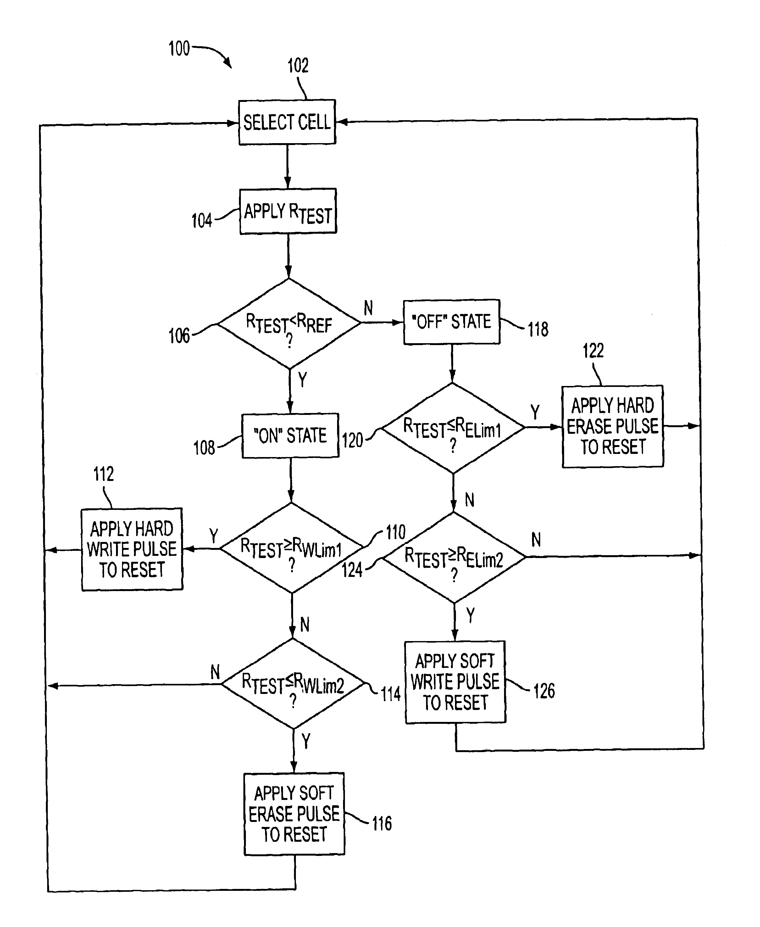
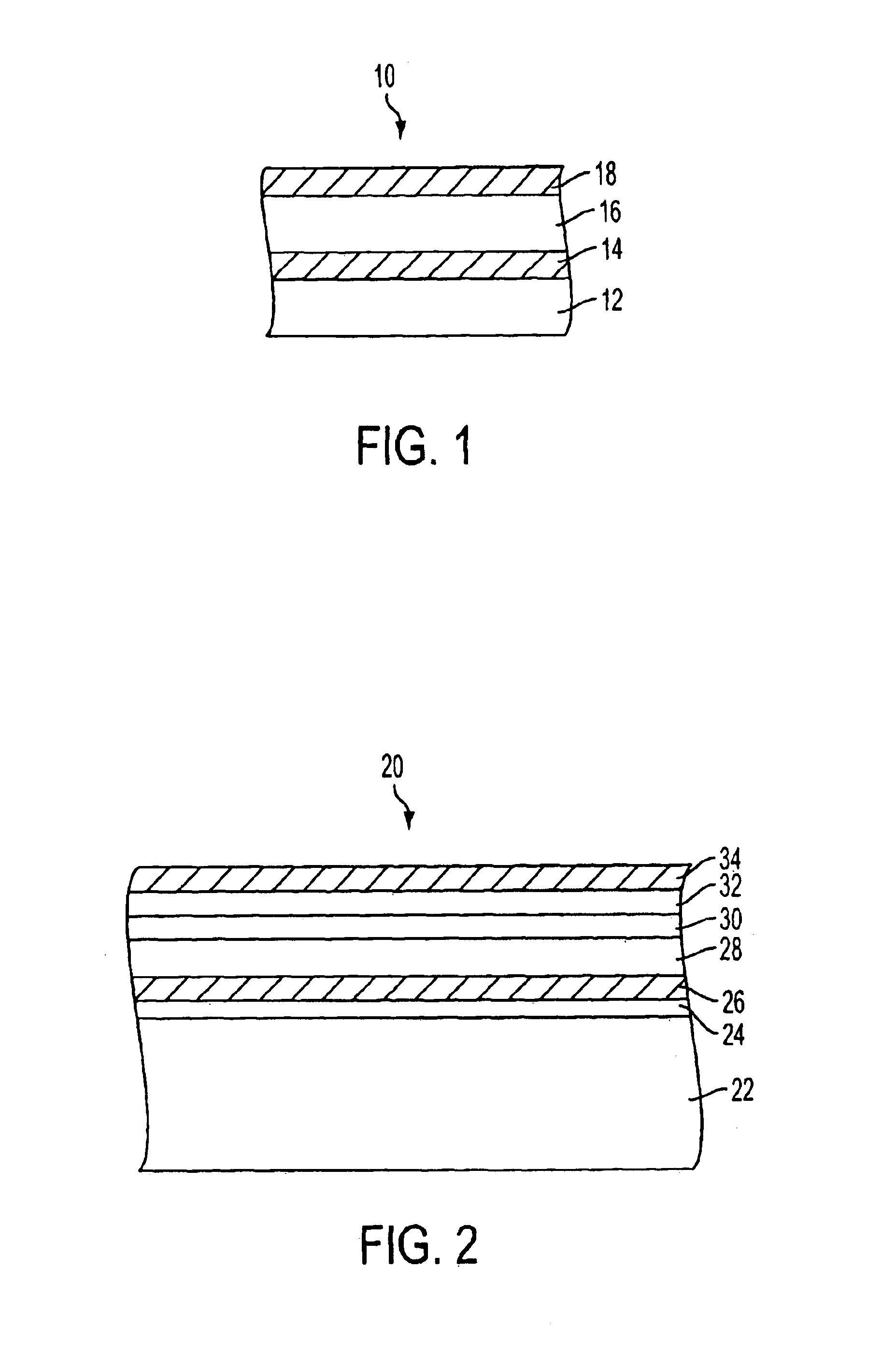
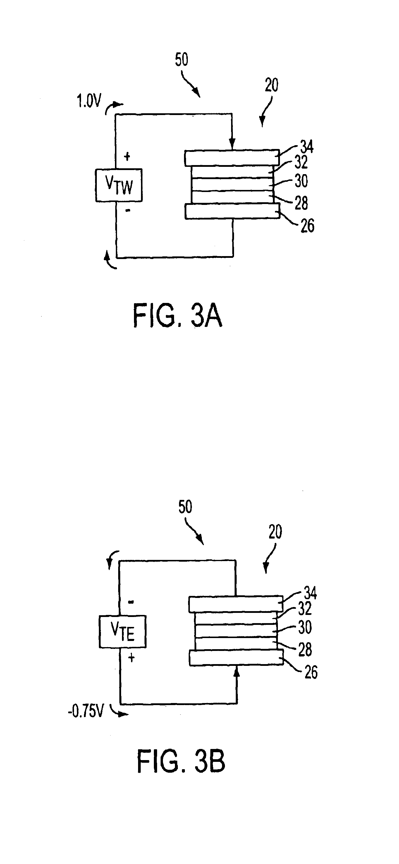
[0061]In the following detailed description, reference is made to various specific structural and process embodiments of the invention. These embodiments are described with sufficient detail to enable those skilled in the art to practice the invention. It is to be understood that other embodiments may be employed, and that various structural, logical and electrical changes may be made without departing from the spirit or scope of the invention.
[0062]The term “substrate” or “wafer” used in the following description are to be understood as interchangeable and may include any supporting structure including, but not limited to, a plastic or a semiconductor substrate that has an exposed substrate surface. Semiconductor substrates should be understood to include silicon, silicon-on-insulator (SOI), silicon-on-sapphire (SOS), doped and undoped semiconductors, epitaxial layers of silicon supported by a base semiconductor foundation, and other semiconductor structures. When reference is made...
PUM
 Abstract
Description
Claims
Application Information