Method of reading memory device in page mode and row decoder control circuit using the same
a memory device and control circuit technology, applied in information storage, static storage, digital storage, etc., can solve the problems of increasing current consumption, cell has to be restored, and entire access time to be delayed, so as to reduce current consumption in page mode
- Summary
- Abstract
- Description
- Claims
- Application Information
AI Technical Summary
Benefits of technology
Problems solved by technology
Method used
Image
Examples
first embodiment
[0039](First Embodiment)
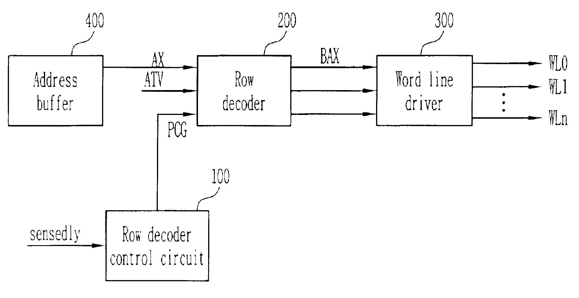
[0040]According to the first embodiment, after a lapse of a certain time period as much as the operation of the bit line sense amplifier is stably performed and the data of the first cell node CN is sufficiently restored, a delay circuit is used in order to disable the word lines. In other words, the delay time is adjusted by stably executing the operation of the first bit line sense amplifier in design and calculating as much time as the data of the cell node is sufficiently restored.
[0041]Preferably, the circuit is constructed to output a sense delay signal (sensedly) and to generate a precharge control signal (pcg) based on the output. The circuit can also be implemented so that the word line enabled by the precharge control signal (pcg) is disabled. Accordingly, the circuit can be implemented by outputting the precharge control signal (pcg) after a lapse of an adequate time period as much as the data of the first cell is read and restored thorough control...
second embodiment
[0051](Second Embodiment)
[0052]FIG. 12 is a block diagram illustrating the whole circuit having a row decoder control circuit 500 according to a second embodiment of the present invention. FIG. 13 is a detailed circuit diagram illustrating the control circuit 500 according to the second embodiment of the present invention. Description will now be given on the basis of the difference of the second embodiment from the first embodiment. A row decoder control circuit 500 produces a precharge control signal (pcg) using an address transition detector signal (ATDB_P) generated through a page address (AP). Through this, the circuit is constructed so that the operation of the bit line sense amplifier is stably performed and the word line is disabled after a lapse of a certain time period as much as the data of the first cell node CN will be sufficiently restored. In other words, after the operation for reading the first cell node is finished, the circuit uses the address transition detector ...
PUM
 Abstract
Description
Claims
Application Information


