High density modular backplane connector for fiber optics

a fiber optics and backplane technology, applied in optics, instruments, optical light guides, etc., can solve the problems of limiting the distribution potential of the system, the hardware of the optical connecting device needs to be sufficiently small, and the construction of the connector is relatively complex

Active Publication Date: 2005-08-23
FURAKAWA ELECTRIC NORTH AMERICA INC
View PDF4 Cites 42 Cited by
  • Summary
  • Abstract
  • Description
  • Claims
  • Application Information

AI Technical Summary

Benefits of technology

[0009]The standard LC connector includes a resilient latching arm having latching lugs on either side thereof for latching the connector to a standard adapter. In accordance with the present invention, the latching arm is shortened and has a lateral latching face on its distal end termination, and the latching lugs are removed. Thus, when the connector is inserted into the housing opening so that the latching arm rides in a channel, the connector rests upon the shelf and the latching ann, being resilient, intrudes into the latching aperture, thereby latching the connector in the housing. In the embodiment discussed herein, the eight connectors may be inserted into the upper opening and eight in the lower and latched in place, with the sides of each of the connectors contacting the sides of adjacent connectors. Thus, there are no walls, ribs, or septa separating connectors fr

Problems solved by technology

Nevertheless, distribution equipment is still needed to route optical signals to the same pre-existing locations, and this means that optical connecting hardware needs to be sufficiently small to accommodate large numbers of individual fiber connections.
Thus, while high speed and large bandwidth are achievable, the amount of space, or “real estate” available for making necessary connections of the fiber is limited, thereby limiting the distribution potential of the system.
It is therefore a challenging task to provide a number of optical devices on a plug-in optical circuit board that accurately mate with a corresponding number of stationary optical connectors.
Optical devices are known that might be adapted to mount on an optical circuit board, but their construction is relatively complex and/or their attachment to an optical circuit board requires exp

Method used


Image

  • High density modular backplane connector for fiber optics
  • High density modular backplane connector for fiber optics
  • High density modular backplane connector for fiber optics

Examples


Embodiment Construction

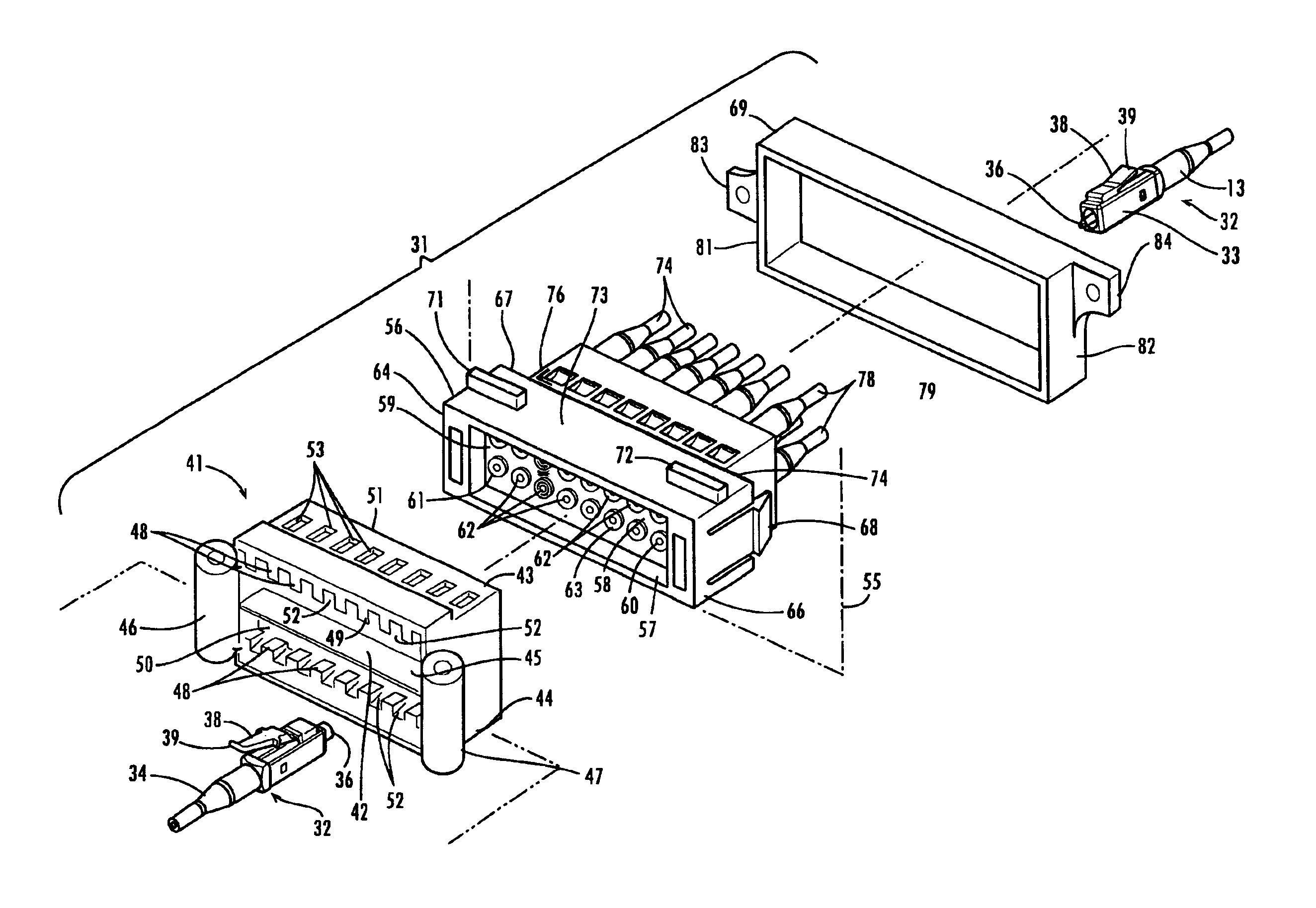
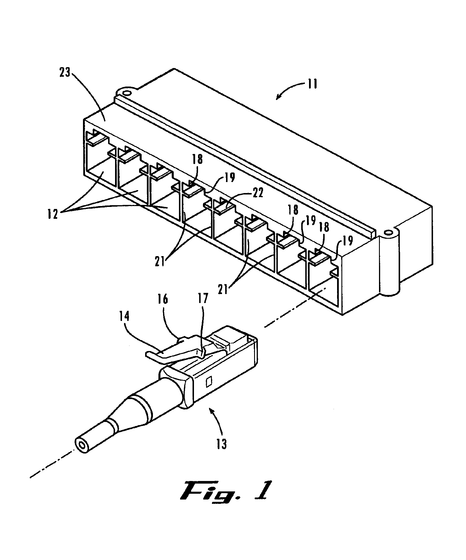
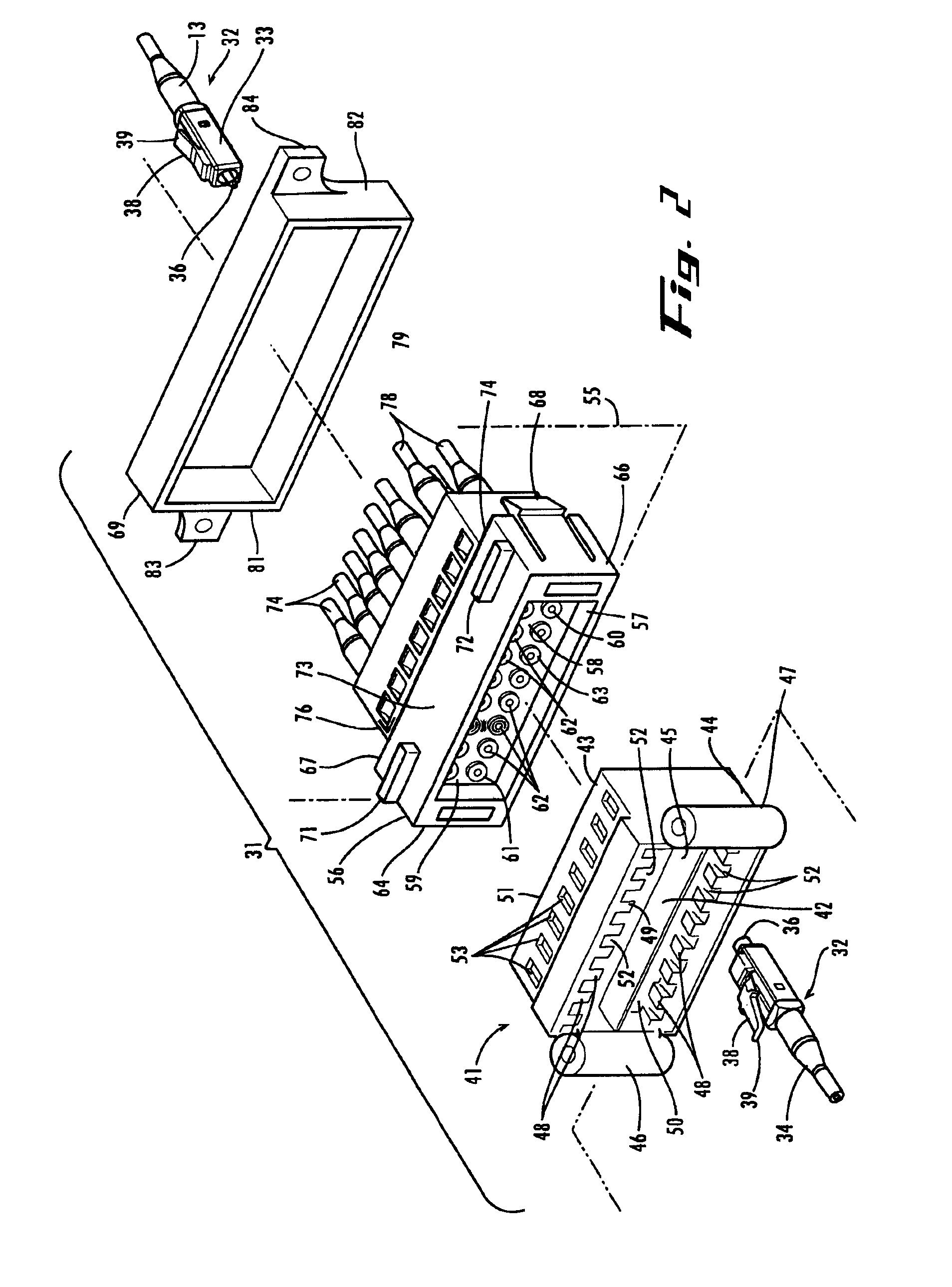
[0020]FIG. 1 illustrates an eight apertured adapter 11, which generally is mounted on the backplane panel, not shown, as is illustrated in U.S. Pat. No. 6,402,393B1 of Grimes, et al., the disclosure of which is incorporated herein by reference, but which may, instead, be mounted on the PCB (not shown), provided the backplane has mounted thereon a mating structure. Each of the eight apertures 12 is adapted to receive a standard LC connector 13 which has a resilient cantilevered latching arm 14, equipped with first and second latching lugs 16 and 17 which are adapted to latch to latching ridges 18 and 19 extending from the walls 21 of each of the apertures 12 when the connector 13 is inserted therein. In the case where adapter 11 is mounted on the backplane, the connectors 13 are mounted on the PCB in a manner such as is shown in the Grimes et al patent, spaced to match the spacing of the apertures 12 in adapter 11. As can be seen in FIG. 1, each of the apertures 12 has a channel 22 t...


PUM


Abstract

A high density panel mounting assembly has a first connector housing having first and second arrays of channels for receiving modified connectors, separated by a shelf. An adapter assembly for receiving the ferrules of the connectors has an interior wall having first and second arrays of bored projections forming sleeves for receiving the connector ferrules. The adapter assembly has a second connector housing substantially identical with the first connector housing mounted to or integral with the rear of the adapter housing for receiving individual connectors. Each of the connector housings has an array of apertures along the top and bottom surfaces for latching the connectors in place. Each of the connectors has a resilient latching arm having a distal end having a latching surface thereon which bears against the end of its corresponding aperture to latch the connector in place within the connector housing. The first and second connector housings each receives the connectors in an aperture, the width of which is substantially equal to the sum of the widths o the connectors so that the connectors, when in place, bear against each other to prevent lateral displacement thereof.

Description

FIELD OF THE INVENTION[0001]This invention relates to a high density panel mounting assembly for interconnecting optical circuit boards with optical connectors arrayed on a mounting panel or backplane.BACKGROUND OF THE INVENTION[0002]For a variety of reasons, modem communication equipment is now being designed to process data at progressively higher speeds. Perhaps the most significant reason relates to the need to transfer video information between computers. Such data transfer has grown exponentially in recent years, and no decrease in growth is anticipated in the foreseeable future. In order to handle this growth, only optical circuitry appears capable of meeting the demand because of the enormous bandwidth that an optical fiber can provide. Nevertheless, distribution equipment is still needed to route optical signals to the same pre-existing locations, and this means that optical connecting hardware needs to be sufficiently small to accommodate large numbers of individual fiber ...

Claims


Application Information

Patent Timeline
IPC IPC(8): G02B6/38
CPCG02B6/3825G02B6/3897G02B6/3893
Inventor ANDERSON, JERRY M.ANDREWS, SCOTT R.JONES, SEAN L.LAMPERT, NORMAN R.SANDELS, GREGORY A.
Owner FURAKAWA ELECTRIC NORTH AMERICA INC
Why Eureka
Try Eureka