Method of manufacturing semiconductor device featuring formation of conductive plugs

a technology of semiconductor devices and plugs, applied in semiconductor devices, semiconductor/solid-state device details, electrical apparatus, etc., can solve problems such as short circuits, unwanted electrical connections or short circuits, and achieve the effect of increasing the overlay tolerance of metal interconnects

Inactive Publication Date: 2005-08-23
NAN YA TECH
View PDF6 Cites 2 Cited by
  • Summary
  • Abstract
  • Description
  • Claims
  • Application Information

AI Technical Summary

Benefits of technology

[0008]Accordingly, the present invention is to provide a semiconductor device and manufacturing method thereof for increasing overlay tolerance of metal interconnects.
[0009]This invention is to provide a semiconductor device and manufacturing method thereof for preventing a short circuit between a contact plug and a neighboring conductive structure.
[0011]In this invention, the contact / via plug is fabricated by combining two sections together, namely, a bottom plug and a top plug. With this setup, the aspect ratio of the contact / via opening in the process of forming the contact / via is very much reduced. Hence, the process of etching out contact / via openings and the deposition of conductive material into the opening thereafter is greatly simplified.
[0012]Because the top plug has a critical dimension smaller than the junction portion of the funnel shaped bottom plug, the alignment tolerance with respect to the bottom plug in the photolithographic process for forming the top plug opening is increased. Furthermore, with the top plug having a smaller critical dimension, the wire lines above the top plugs can have a larger alignment tolerance so that the probability of having a short circuit due to misalignment is lowered considerably.
[0013]In addition, the shoulder chamfer or shoulder recess in the conductive layer of the conductive structure permits the formation of a thicker liner layer in this area. Therefore, the section between the bottom plug and the conductive layer, in particular, between the conductive layer and the shoulder section can have a thicker isolating liner layer for preventing plug / conductive layer short circuit.

Problems solved by technology

Should an alignment error occur, a neighboring conductive structure such as the conductive layer of a gate structure may be exposed leading to a possible short circuit between a subsequently formed contact plug and the conductive structure.
Any minor misalignment will likely lead to an unwanted electrical connection or short-circuit between a metal line 10 and a neighboring plug.

Method used


Image

  • Method of manufacturing semiconductor device featuring formation of conductive plugs
  • Method of manufacturing semiconductor device featuring formation of conductive plugs
  • Method of manufacturing semiconductor device featuring formation of conductive plugs

Examples


Embodiment Construction

[0020]Reference will now be made in detail to the present preferred embodiments of the invention, examples of which are illustrated in the accompanying drawings. Wherever possible, the same reference numbers are used in the drawings and the description to refer to the same or like parts.

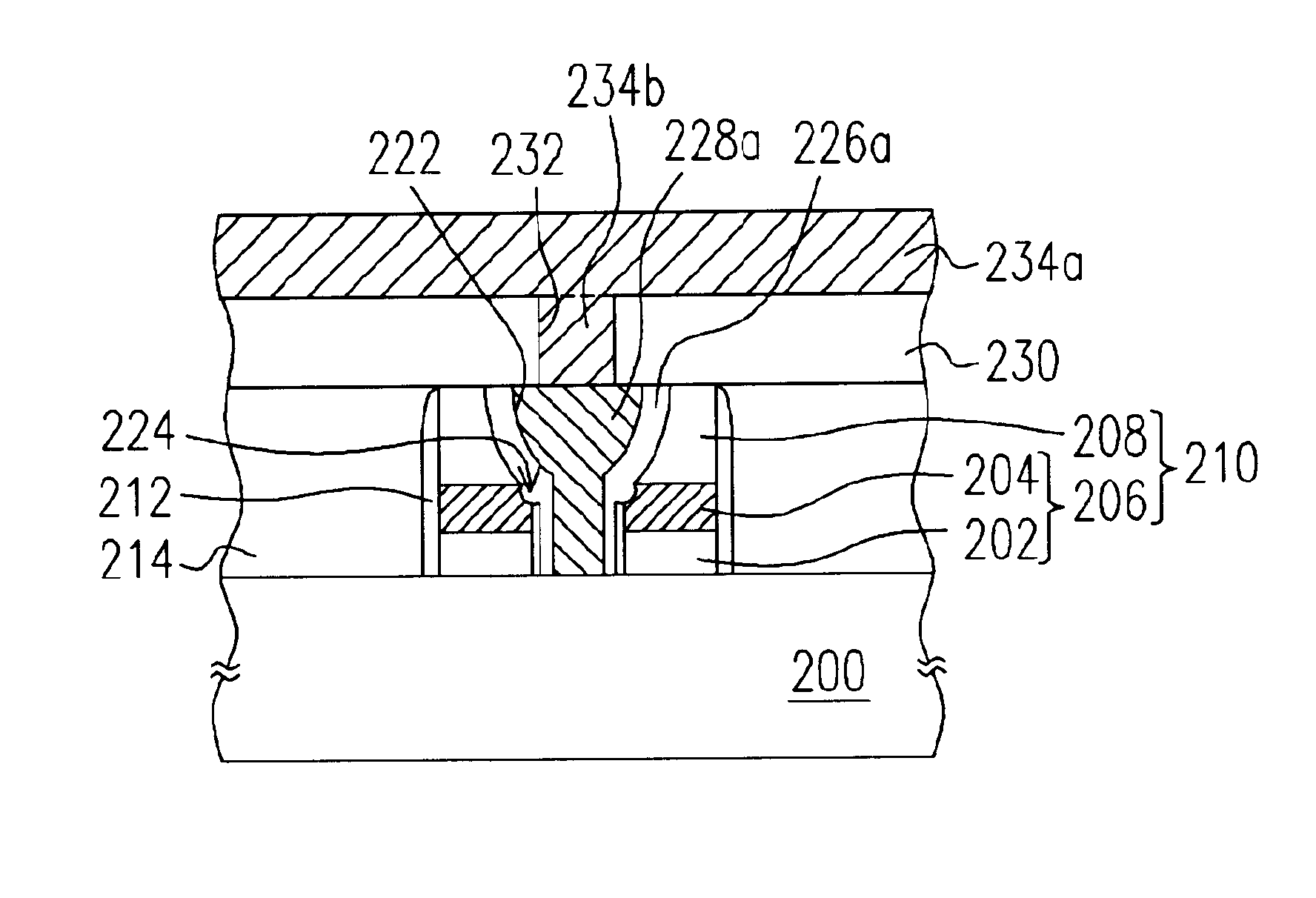
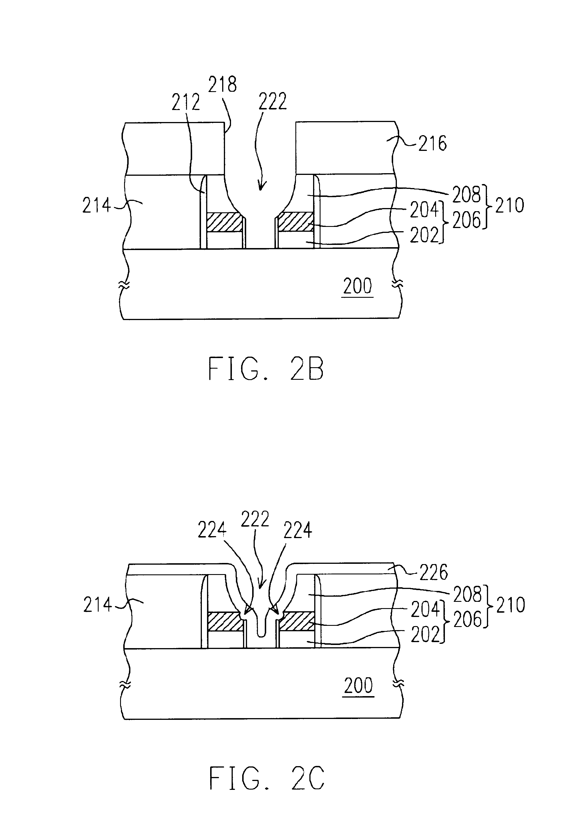
[0021]FIGS. 2A through 2F are schematic cross-sectional views showing the progression of steps for fabricating metal interconnects according to one preferred embodiment of this invention. As shown in FIG. 2A, a plurality of conductive structures 210 is formed over a substrate 200. Each conductive structure 210 at least comprises a conductive layer 206 and a cap layer 208. The conductive layer 206 further comprises a polysilicon layer 202 and a metal silicide layer 204, for example. The cap layer 208 is a silicon nitride layer, for example. Thereafter, spacers 212 are formed on the sidewalls of the conductive structures 210. The spacers 212 are silicon nitride layers formed by performing a chemical va...


PUM


Abstract

A semiconductor device and method of manufacturing the same are disclosed. A conductive structure, spacers and a dielectric layer are formed on a substrate. Thereafter, a portion of the cap layer, a portion of the spacers and a portion of the dielectric layer of the conductive structure are removed to form a funnel-shaped opening. The shoulder section of the conductive layer exposed by the funnel-shaped opening is removed to form a shoulder recess. A liner layer is formed on the sidewall of the funnel-shaped opening and then a bottom plug is formed inside the funnel-shaped opening. Another dielectric layer is formed over the substrate. A top plug is formed in the dielectric layer such that the top plug and the bottom plug are electrically connected. Finally, a wire line is formed over the substrate.

Description

CROSS REFERENCE TO RELATED APPLICATIONS[0001]This application claims the priority benefit of Taiwan application serial no. 92119109, filed on Jul. 14, 2003.BACKGROUND OF INVENTION[0002]1. Field of the Invention[0003]The present invention relates to an integrated circuit and fabricating method thereof. More particularly, the present invention relates to a semiconductor device and method of fabricating the same.[0004]2. Description of the Related Art[0005]Typically, integrated circuit devices are interconnected via metal interconnects. The conventional method of fabricating metal interconnects includes forming a metal plug in a dielectric layer and then forming a metal line over a substrate to connect with the metal plug. FIG. 1 is a top view showing the layout of conventional metal interconnects. As the level of integration for semiconductor devices continues to increase, the aspect ratio of contact openings must be reduced to avoid difficulties encountered while carrying out etching...

Claims


Application Information

Patent Timeline
Patent Type & Authority Patents(United States)
IPC IPC(8): H01L21/70H01L21/8239H01L27/105H01L23/485H01L23/48H01L21/60H01L21/768
CPCH01L21/76804H01L21/76897H01L27/105H01L27/1052H01L23/485H01L2924/0002H01L2924/00H10B99/00
Inventor KUAN, SHIH-FANWU, KUO-CHIEN
Owner NAN YA TECH
Why Eureka
Try Eureka