Spacer with passive components for use in multi-chip modules

a technology of spacers and passive components, applied in the field of integrated circuits, can solve the problems of waste of module internal area, cost of forming a package around multiple dies, and insertion of spacers merely for insulation between active dies, so as to achieve more design freedom and efficient use of the total internal volume of the multi-chip module

Inactive Publication Date: 2005-08-23
NAT SEMICON CORP
View PDF11 Cites 33 Cited by
  • Summary
  • Abstract
  • Description
  • Claims
  • Application Information

AI Technical Summary

Benefits of technology

[0006]In a first embodiment of the present invention, a spacer containing embedded passive components such as resistors, inductors or capacitors is placed between the semiconductor dies bearing active components in a stacked die multi-chip module. These passive components can perform such tasks as noise filtering and / or signal filtering, electro-static discharge (ESD) protection, electromagnetic interference (EMI) protection and similar functions. By moving these functions to the previously inert spacer, the total internal volume of the multi-chip module is used more efficiently and the designers of the active dies have more design freedom, as the enumerated passive functions as well as other similar functions can be effected in the previously inert spacer. Several of the enumerated passive components also require a comparatively large amount of semiconductor die area to fabricate. Moving them to the spacer thus frees up very valuable semiconductor real estate on the active semiconductor dies.

Problems solved by technology

The number of dies in either a horizontal layout multi-chip module or a vertical layout multi-chip module will be constrained by the difficulty of forming connections between the dies, the cost of forming a package around multiple dies, the availability of printed circuit board (“PCB”) realty to mount the finished module and other, similar issues.
Although these known multi-chip modules are adequate for their intended uses, the insertion of spacers merely for insulation between active dies is wasteful of the module's internal area.

Method used


Image

  • Spacer with passive components for use in multi-chip modules
  • Spacer with passive components for use in multi-chip modules
  • Spacer with passive components for use in multi-chip modules

Examples


Embodiment Construction

[0016]In the following description, numerous specific details are set forth in order to provide a thorough understanding of the present invention. It will be understood to one skilled in the art that the present invention may be practiced without some or all of these specific details. In some instances, well known processes have not been described in detail in order not to unnecessarily obscure the present invention.

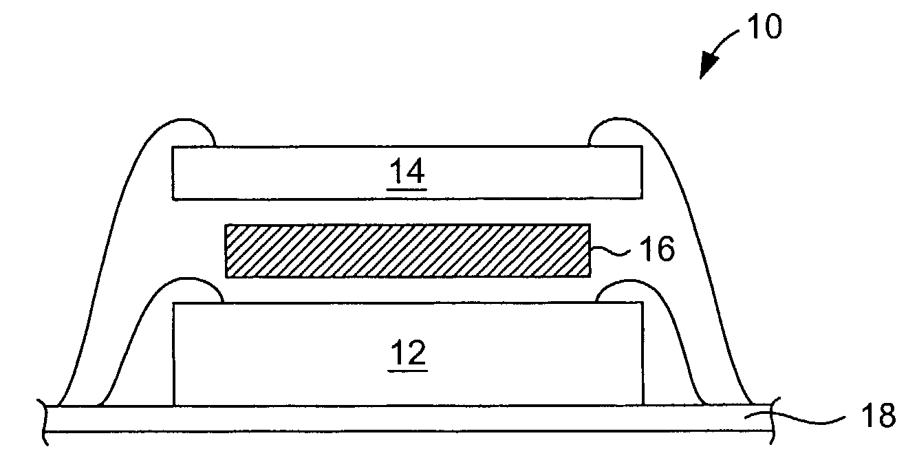
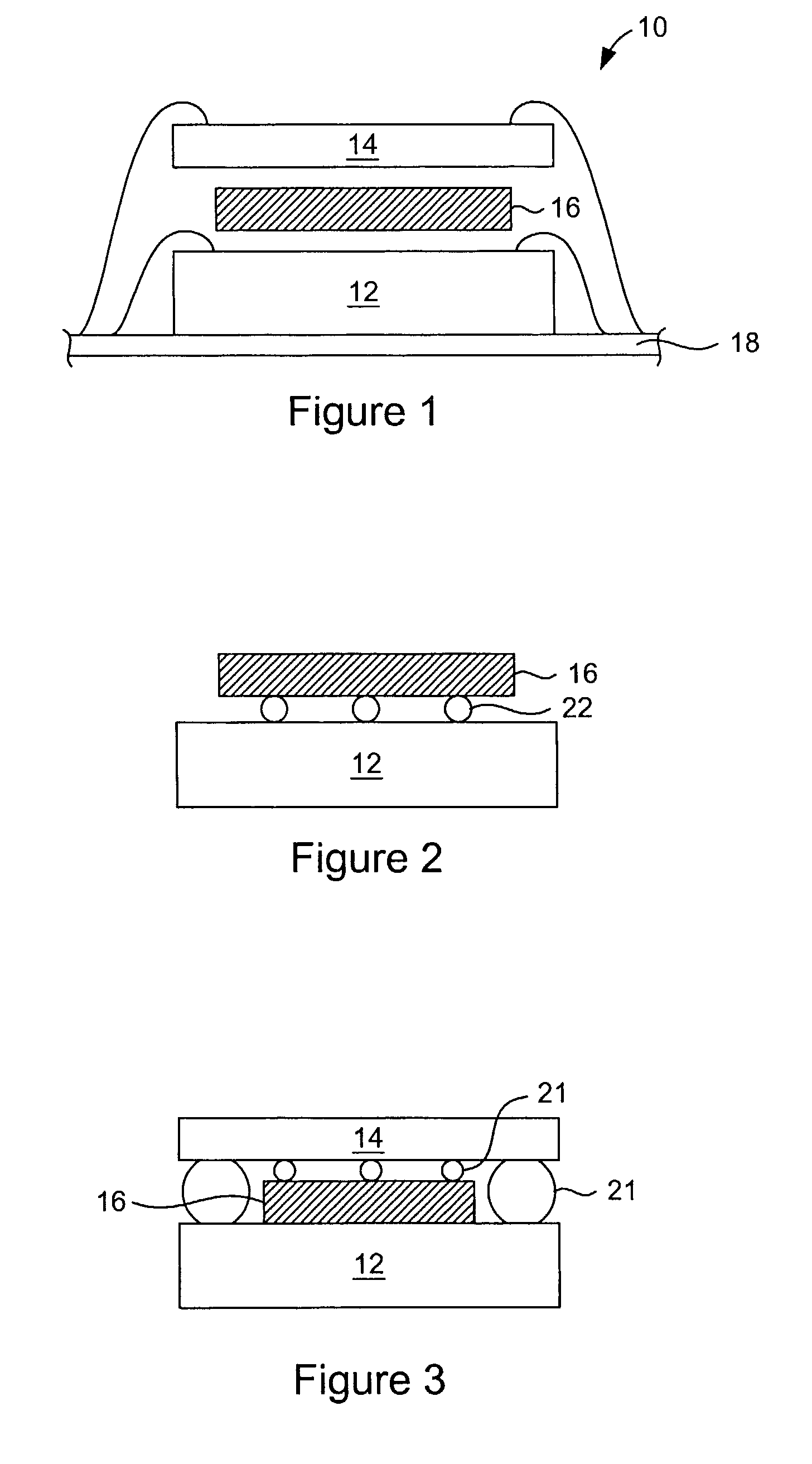
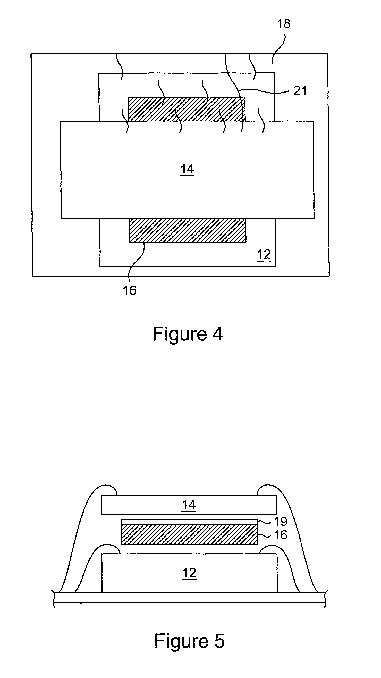
[0017]As shown in FIG. 1, multi-chip module 10 comprises two active dies, respectively 12 and 14, a spacer 16 with embedded passive components coupled, in this first embodiment, to die 12 and metal lead frame 18, upon which stacked dies 12 and 14 and spacer 16 are mounted and to which they are coupled. In this first embodiment, dies 12 and 14 are approximately the same size, with die 12 providing radio-frequency (RF) functionality and die 14 providing baseband functionality.

[0018]The completed multi-chip module would include a molded or cast body, made from any number of...


PUM


Abstract

A method for providing passive circuit functions in a multi-chip module and the multi-chip modules that result from incorporating these function is disclosed. Passive components such as resistors, capacitors and inductors are fabricated on or within a non-conductive spacer. The spacer is then placed between two active semiconductor dies and coupled electrically to either one or both of the dies. In this manner, area of the active dies that would normally have to be used for such passive components is freed for other uses and the spacer, which was already required in multi-chip modules, is endowed with extra functionality. In another embodiment, one or both surfaces of the spacer are coated with a conductive metal and the passive components are located within the spacer. In this embodiment, the spacer provides electromagnetic interference protection between the active dies.

Description

BACKGROUND OF THE INVENTION[0001]This invention relates to the field of integrated circuits (ICs). More particularly, it relates to multi-chip modules and their fabrication.[0002]Multi-chip modules are known within the semiconductor fabrication industry. In a multi-chip module, several semiconductor dies, each die consisting of active and passive components, are coupled together and incorporated into a single completed IC package. For purposes of this invention, any IC containing two or more separate semiconductor dies will be called a multi-chip module. Examples of known multi-chip modules include a first semiconductor die with digital circuitry coupled together with a semiconductor die having analog circuitry, the two dies together being mounted within a single IC package. Similarly, digital semiconductor memory dies can be coupled together in whatever multiple is practical (e.g. 2*64 Mbit) and placed within a single IC package to create a large multi-chip module memory that is la...

Claims


Application Information

Patent Timeline
Patent Type & Authority Patents(United States)
IPC IPC(8): H01L23/02H01L23/552H01L25/065
CPCH01L23/552H01L25/0657H01L2224/16H01L2224/48091H01L2225/0651H01L2225/06555H01L2225/06562H01L2225/06572H01L2924/01078H01L2924/01079H01L2924/15311H01L2924/1532H01L2924/19041H01L2924/3025H01L2924/00014H01L24/48H01L2924/14H01L2924/00H01L2224/45099H01L2224/45015H01L2924/207
Inventor PODDAR, ANINDYAPRABHU, ASHOK S.
Owner NAT SEMICON CORP
Why Eureka
Try Eureka