300MM single stackable film frame carrier

a film frame carrier and film frame technology, applied in the field of single, stackable film frame carriers for semiconductors, can solve the problems of reducing the likelihood that the film frame carrier will be dislodged, and achieve the effects of stable horizontal orientation, improved economic benefits, and reduced likelihood of wafer and chip damage during handling

Inactive Publication Date: 2005-01-04
ENTEGRIS INC
View PDF10 Cites 23 Cited by
  • Summary
  • Abstract
  • Description
  • Claims
  • Application Information

AI Technical Summary

Benefits of technology

Hence, film frame carriers configured to be horizontally stacked after being loaded with semiconductor wafers offer enhanced economy and a greatly decreased likelihood of wafer and chip damage during handling, storage, and transportation.
It is one advantage of the present carrier that wafers may be stored, transported, a

Problems solved by technology

The practice of stacking and interlocking (mating) the film frame carriers with interposed film frames therebetween also decreas

Method used


Image

  • 300MM single stackable film frame carrier
  • 300MM single stackable film frame carrier
  • 300MM single stackable film frame carrier

Examples


Embodiment Construction

Any references to such relative terms as inboard and outboard, upper and lower, and the like, are intended for convenience of description and are not intended to limit the present invention or its components to any one positional or spatial orientation.

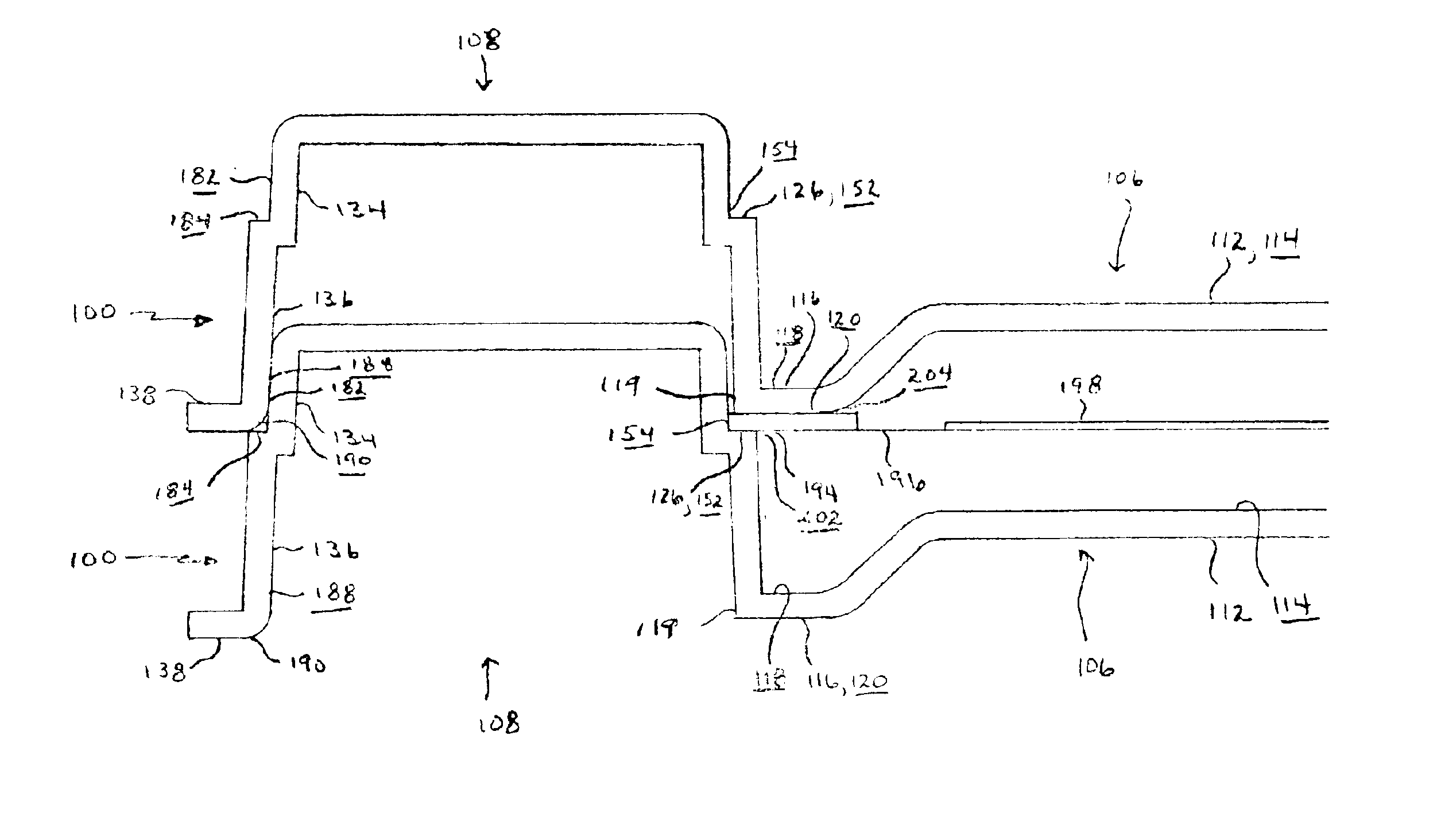
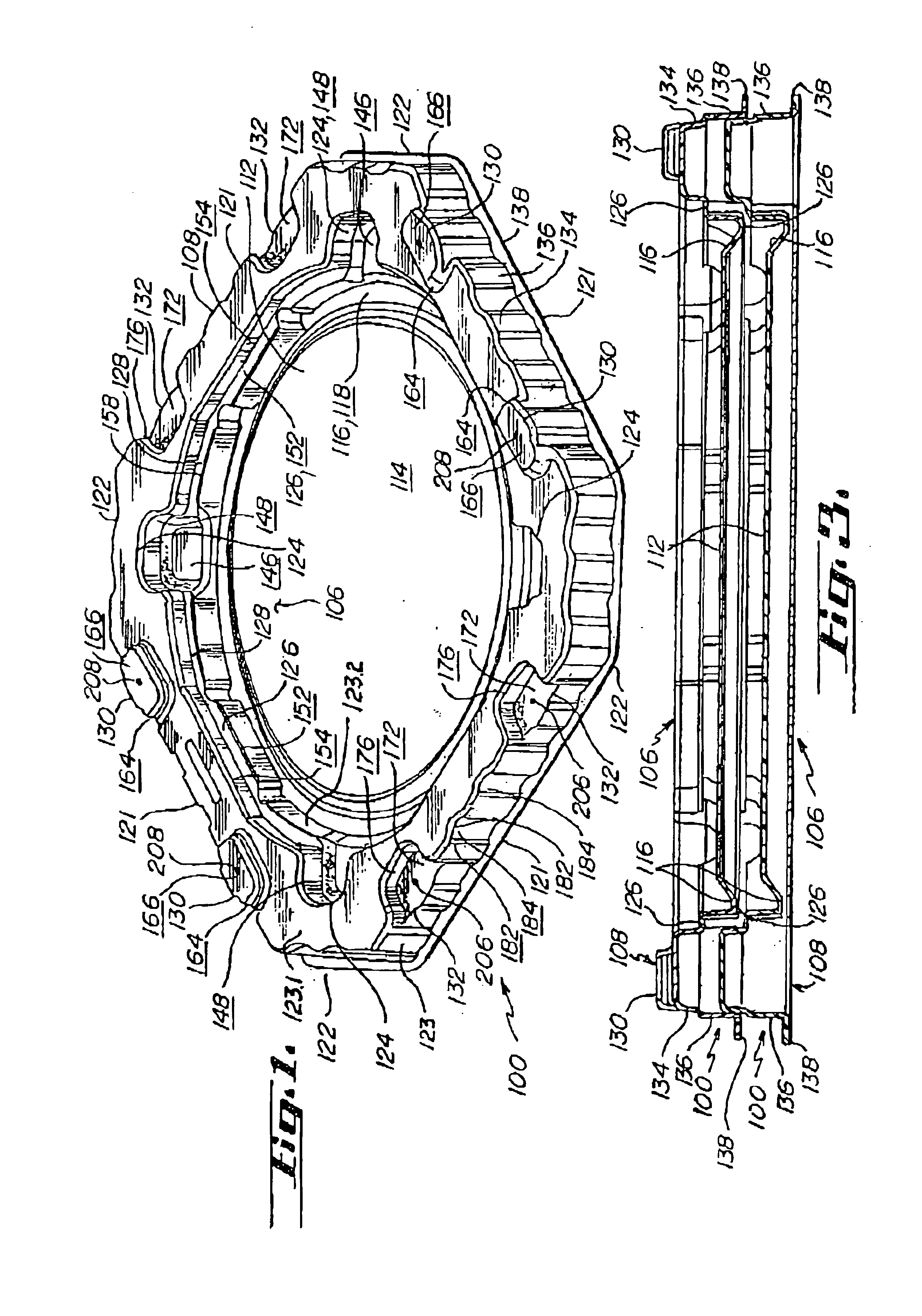
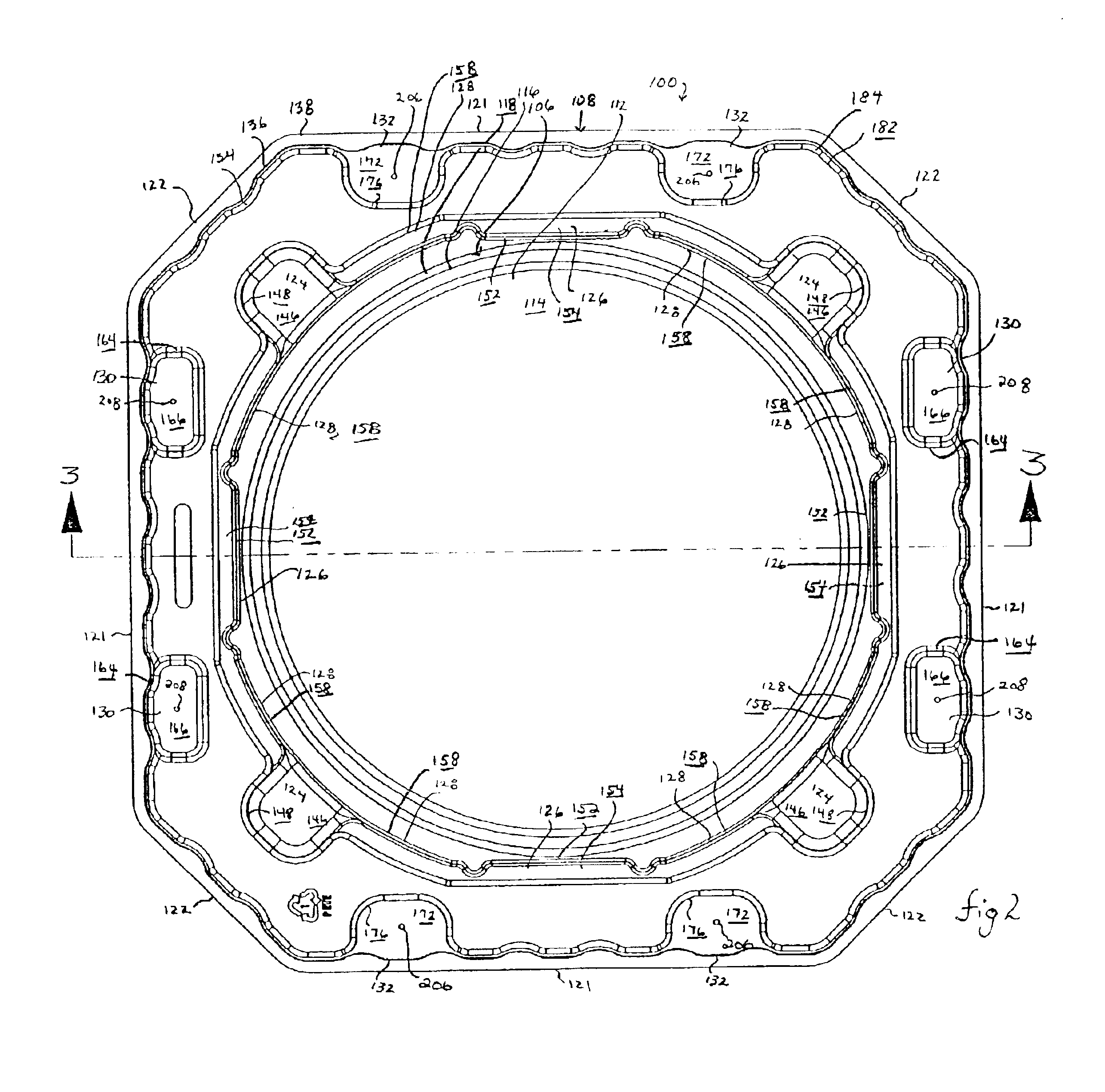
One embodiment of the present single stackable film frame carrier is shown in the figures generally at 100. One suitable material for making the present film frame carrier is polyethylene terephthalate glycol between about 0.075 and 0.125 inch in thickness. However, it is recognized that several materials and thicknesses may be suitable for other embodiments. A conductor such as carbon may also be present in the synthetic resin used to make the present film frame carrier, for example, if static electricity dissipation is desired. The present film frame carrier is substantially unitary (or otherwise integral), having been thermally formed or vacuum molded from a single sheet of synthetic resin in one embodiment. However, the present fi...


PUM

PropertyMeasurementUnit
Thicknessaaaaaaaaaa
Thicknessaaaaaaaaaa
Structureaaaaaaaaaa

Abstract

An interlockable film frame carrier has central and peripheral portions for securely storing a film frame, the film frame supporting a film, a semiconductor wafer disposed on the film. The central portion has structure for supporting the semiconductor wafer and for allowing access to a lower surface of the stored film frame. The peripheral portion of the film frame carrier includes structure for supporting a peripheral portion of the film frame and matable stacking members. When the film frame is stored, two film frame carriers are interlocked by mating the stacking members. It is emphasized that this abstract is provided to comply with the rules requiring an abstract that will allow a searcher or other reader to quickly ascertain the subject matter of the technical disclosure. It is submitted with the understanding that it will not be used to interpret or limit the scope or meaning of the claims. 37 CFR §1.72 (b).

Description

BACKGROUND1. Field of the InventionThis invention relates to carriers for semiconductors. In particular, this invention relates to single, stackable film frame carriers for semiconductors.2. Background of the InventionThe present invention relates to thermal-formed, stackable carriers for film frames. Film frames are generally stainless-steel with a film extending across the film frame. The film has an adhesive on one side thereof. After being processed, a round semiconductor wafer is placed on the film. After being positioned on the film, the semiconductor wafer may be sectioned into individual pieces (e.g., chips), transported for further processing, or stored. The semiconductor processing industry is using larger and thinner wafers. These larger and thinner wafers present processing, transportation, and storage handling problems due to their greater fragility. To this end, conventional wafer carriers have often proven unacceptable for these larger and thinner wafers. The addition...

Claims


Application Information

Patent Timeline
IPC IPC(8): H01L21/67H01L21/673B65D85/86B65D21/02H01L21/683
CPCH01L21/67346Y10S206/821H01L21/68
Inventor NIGG, JAMESZABKA, MICHAEL
Owner ENTEGRIS INC
Why Eureka
Try Eureka