NAND-type flash memory devices and methods of fabricating the same

a flash memory and nano-type technology, applied in the field of nano-type flash memory devices, can solve the problems of current directly affecting access time, and achieve the effects of low resistance, low aspect ratio of bit line contact holes, and low resistan

Inactive Publication Date: 2005-08-30
SAMSUNG ELECTRONICS CO LTD
View PDF10 Cites 30 Cited by
  • Summary
  • Abstract
  • Description
  • Claims
  • Application Information

AI Technical Summary

Benefits of technology

[0014]It is therefore a feature of the present invention to provide a NAND-type flash memory device having low resistance in a common source line as well as low aspect ratio of the bit line contact holes. It is another feature of the present invention to provide methods of fabricating a NAND-type flash memory device, which can minimize the aspect ratio of the bit line contact holes and the resistance of the common source line.
[0017]In one embodiment, the common source line is formed of a doped polysilicon layer and / or a refractory metal polycide layer in order to reduce the resistance of the common source line. Also, the top surface of the common source line may be even with or lower than that of the first interlayer insulating layer.

Problems solved by technology

This is because the cell current directly affects access time of the flash memory device.

Method used


Image

  • NAND-type flash memory devices and methods of fabricating the same
  • NAND-type flash memory devices and methods of fabricating the same
  • NAND-type flash memory devices and methods of fabricating the same

Examples


Embodiment Construction

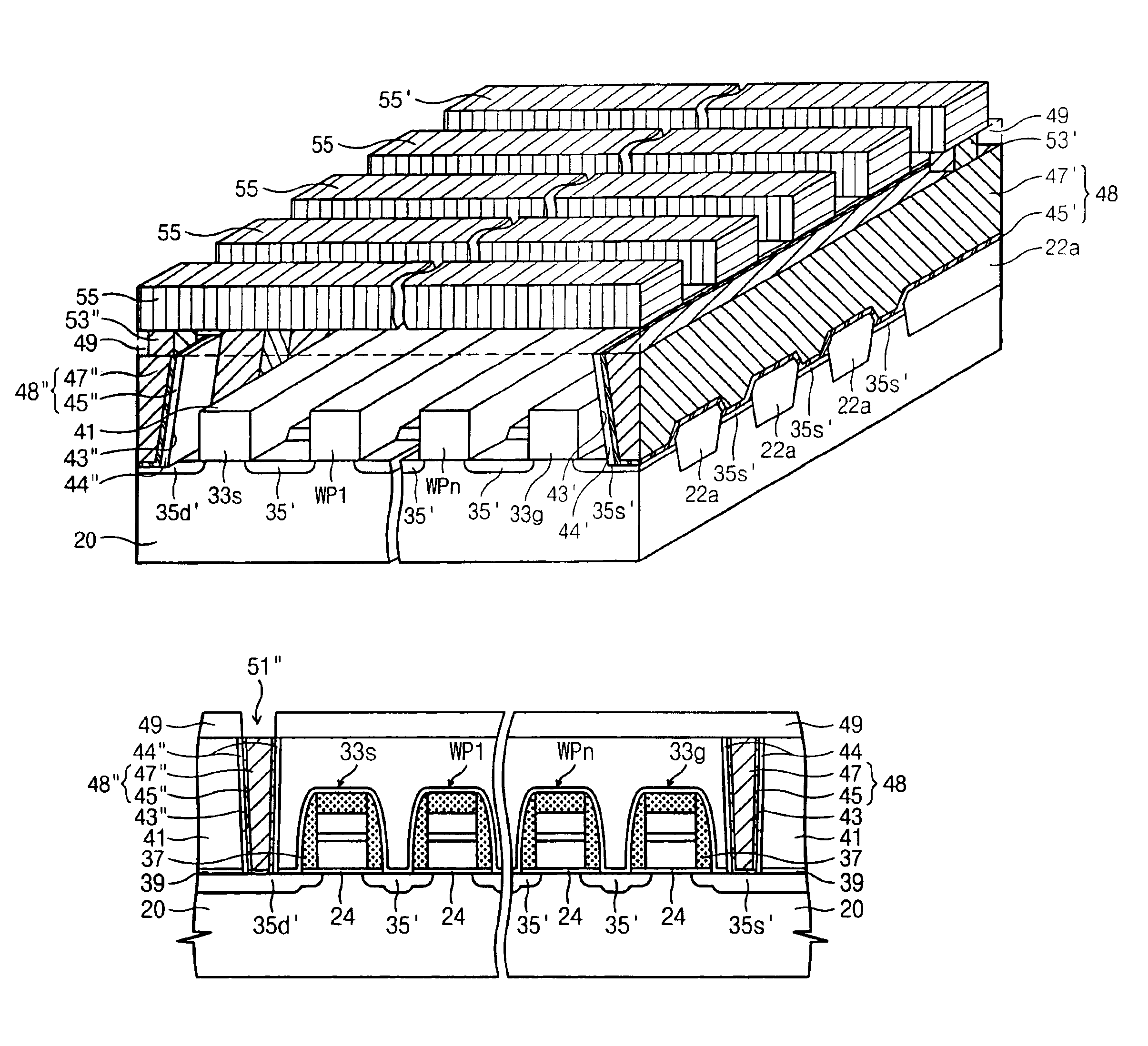
[0050]The present invention will now be described hereinafter with reference to the accompanying drawings, in which preferred embodiments of the invention are shown. This invention may, however, be embodied in many different forms and should not be construed as limited to the embodiments set forth herein. Rather, these embodiments are provided so that this disclosure will be thorough and complete, and will fully convey the scope of the invention. In the drawings, the thickness of layers and regions are exaggerated for clarity. It will also be understood that when a layer is referred to as being on another layer or substrate, it can be directly on the other layer or substrate, or intervening layers may also be present.

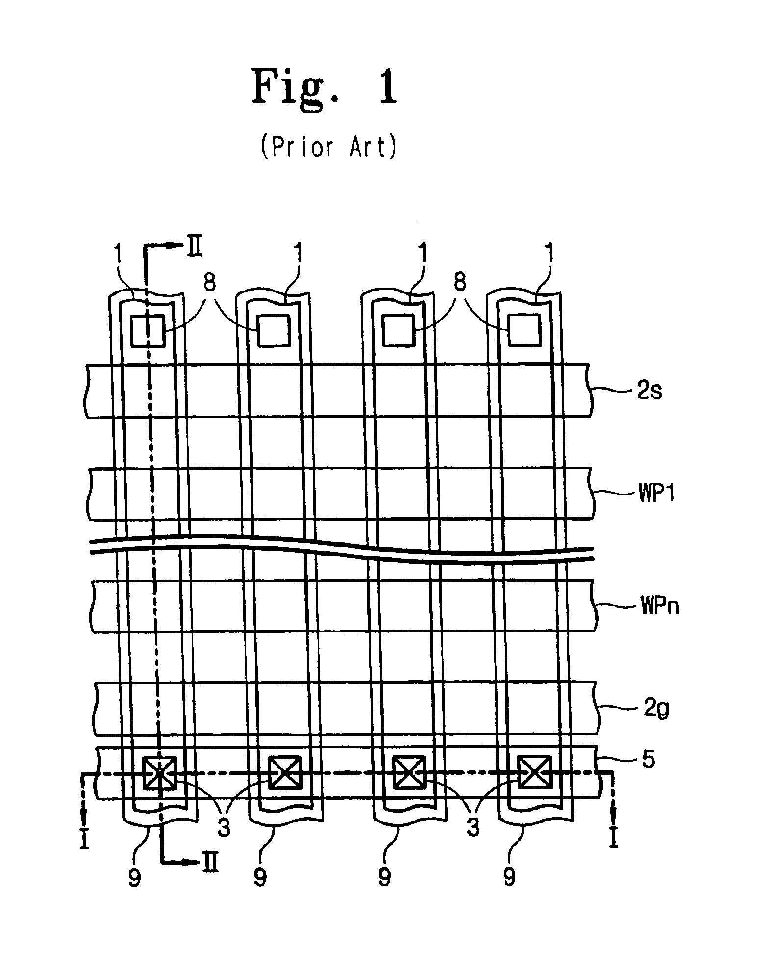
[0051]Referring to FIG. 3A, a cell array region of a NAND-type flash memory device includes a plurality of strings, for example, first to fourth strings S1, S2, S3 and S4. Here, each string includes a string selection transistor SST, a plurality of cell transistors C1 t...


PUM


Abstract

NAND-type flash memory devices and methods of fabricating the same are provided. The NAND-type flash memory device includes a plurality of isolation layers running parallel with each other, which are formed at predetermined regions of a semiconductor substrate. This device also includes a string selection line pattern, a plurality of word line patterns and a ground selection line pattern which cross over the isolation layers and active regions between the isolation layers. Source regions are formed in the active regions adjacent to the ground selection line patterns and opposite the string selection line pattern. The source regions and the isolation layers between the source regions are covered with a common source line running parallel with the ground selection line pattern.

Description

RELATED APPLICATIONS[0001]This application is a continuation-in-part of U.S. application Ser. No. 10 / 087,330, filed Mar. 1, 2002, now U.S. Pat. No. 6,797,570, which ia a divisional of U.S. application Ser. No. 09 / 678,917, filed on Oct. 4, 2000, now U.S. Pat. No. 6,376,876, which relies for priority upon Korean Patent Application No. 2000-2039, filed on Jan. 17, 2000, the contents of which are herein incorporated by reference in their entirety.[0002]This application also claims priority from Korean Patent Application No. 2004-45967, filed on Jun. 21, 2004, the contents of which are herein incorporated by reference in their entirety.FIELD OF THE INVENTION[0003]This invention relates to semiconductor device and methods of fabricating the same and, more particularly, to NAND-type flash memory devices and methods of fabricating the same.BACKGROUND OF THE INVENTION[0004]Non-volatile memory devices such as flash memory devices do not lose data stored in their memory cells when the electric...

Claims


Application Information

Patent Timeline
Patent Type & Authority Patents(United States)
IPC IPC(8): H01L29/78H01L29/788H01L29/66H01L21/768H01L21/8247H01L27/115
CPCH01L27/115H01L27/11521H01L27/11524H01L21/76802H10B69/00H10B41/30H10B41/35
Inventor SHIN, KWANG-SHIKPARK, KYU-CHARNOH, HEUNG-KWUNHUR, SUNG-HOISONG, SANG-BINCHOI, JUNG-DAL
Owner SAMSUNG ELECTRONICS CO LTD
Why Eureka
Try Eureka