Semiconductor device connecting structure, liquid crystal display unit based on the same connecting structure, and electronic apparatus using the same display unit

a technology of liquid crystal display unit and semiconductor device, which is applied in the direction of semiconductor device details, semiconductor/solid-state device details, instruments, etc., can solve the problems of complex process management, unstable electrical connection conditions, and higher component cost and manufacturing costs

Inactive Publication Date: 2005-09-06
TCL CHINA STAR OPTOELECTRONICS TECH CO LTD
View PDF26 Cites 32 Cited by
  • Summary
  • Abstract
  • Description
  • Claims
  • Application Information

AI Technical Summary

Benefits of technology

[0009]According to this connecting structure, the space(s) is specially made in the bonding material when conducting the adhesion between the semiconductor device and the substrate, and absorb the deformation of the semiconductor device and others, changing freely in shape in response to the deformation of the substrate or the semiconductor device. In consequence, even in the case of the deformation of the semiconductor device or the substrate, it is possible to prevent excessive loads from applying on the electrode portions of the semiconductor device, so that the electrical connecting condition of the semiconductor device can be maintained steadily in good condition.
[0010]The space(s) is formed in the bonding material by pressurizing an IC with a pressurizing head ahd by heating at the same time as described below. When the temperature of the pressurizing head is given to the bonding material, the viscosity of the bonding material rapidly decreases to flow out to the external. In this way the space(s)can be formed. Thus, by forming the space(s) in the bonding material, it is possible to relieve the deformation of the semiconductor device or the substrate.
[0018]Preferably, the space rate to the adhesive assumes between 5% and 70%, more preferably between 10% and 30%. This is because, in the case that the space rate is below 5%, it is impossible to absorb the deformation (or stress) of the semiconductor device or the substrates On the contrary, when it assumes more than 70%, the reliability of the connection between the semiconductor device and the substrate (particularly, the terminals formed on the substrate) goes down. Accordingly, if the space(s) is formed at the rate of 5% to 70%, the connection reliability can be obtained. More preferably, if the space rate is set to between 10% and 30%, the structure with improved connection reliability can be formed.
[0020]Furthermore, in accordance with the present invention, a feature of a connecting method of joining a semiconductor device onto a substrate is that a bonding layer is placed in between the substrate and the semiconductor device to join them to each other, and a pressurizing head heated up to a high temperature is pressed against the semiconductor device to pressurize and heat the mentioned bonding layer for joining the substrate to the semiconductor device, and a space(s) is formed in the mentioned bonding layer. With this construction, the deformation of the semiconductor device or the substrate can be reduced by the space(s) and a connecting structure with a higher reliability can be obtained. In addition, the bonding layer is made from an epoxy-based adhesive.
[0022]As mentioned above, it is preferable that the space rate to the adhesive is set to reach 5% to 70%, more preferably 10% to 30%, so that the semiconductor device and the electrode terminals formed on the substrate can be connected with a high reliability.

Problems solved by technology

As a result, the electrical connecting conditions can become unstable.
In addition, for avoiding such problems, the pressure-joining conditions for the liquid crystal driving IC are required to be severely managed within a small tolerance.
As a result, a complicated process management is demanded.
However, in the case of this prior connecting structure, it is required to provide the flexible bonding layer for exclusive use for the purpose of taking the cushioning action, which leads to higher component cost and manufacturing cost.

Method used


Image

  • Semiconductor device connecting structure, liquid crystal display unit based on the same connecting structure, and electronic apparatus using the same display unit
  • Semiconductor device connecting structure, liquid crystal display unit based on the same connecting structure, and electronic apparatus using the same display unit
  • Semiconductor device connecting structure, liquid crystal display unit based on the same connecting structure, and electronic apparatus using the same display unit

Examples


Embodiment Construction

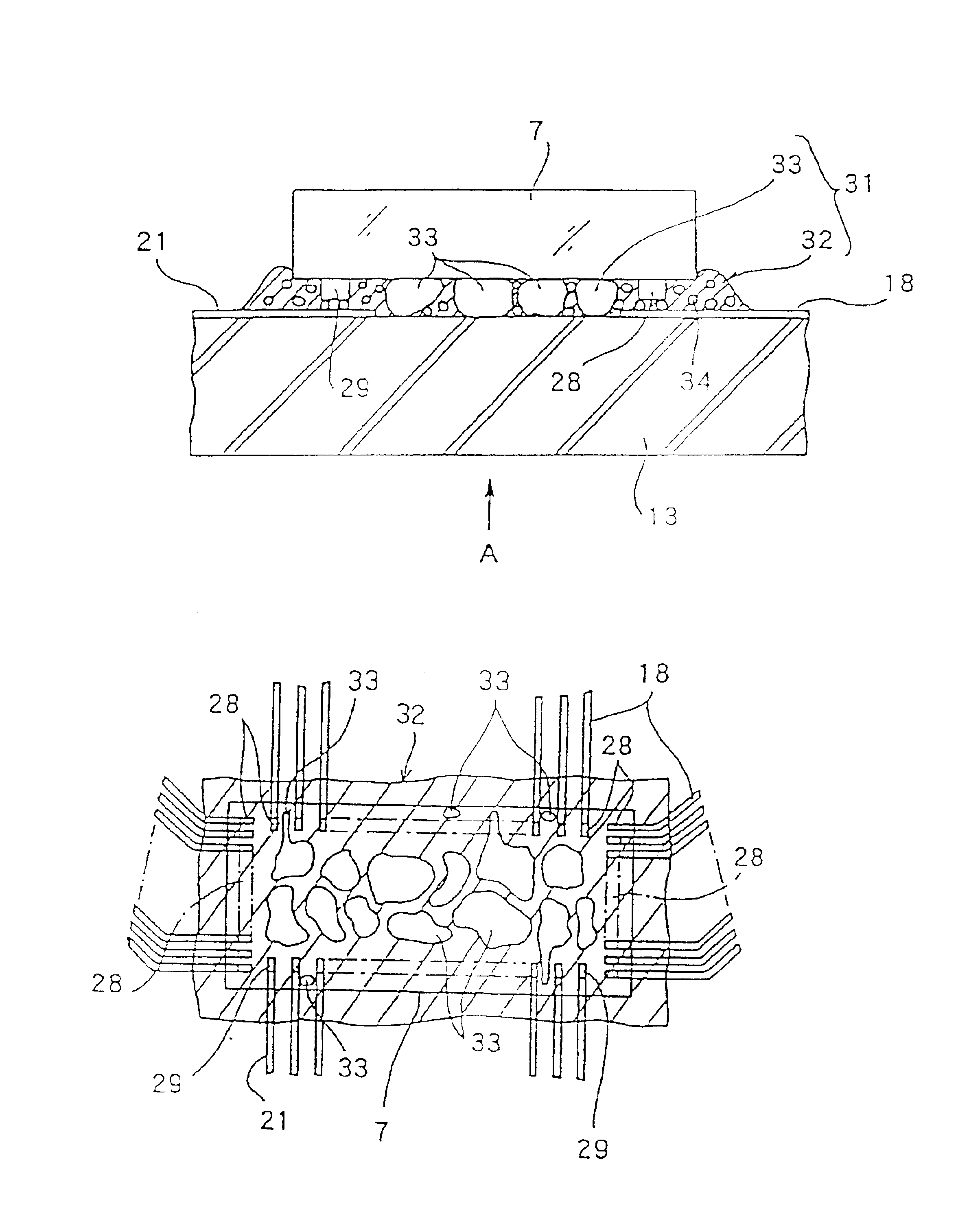
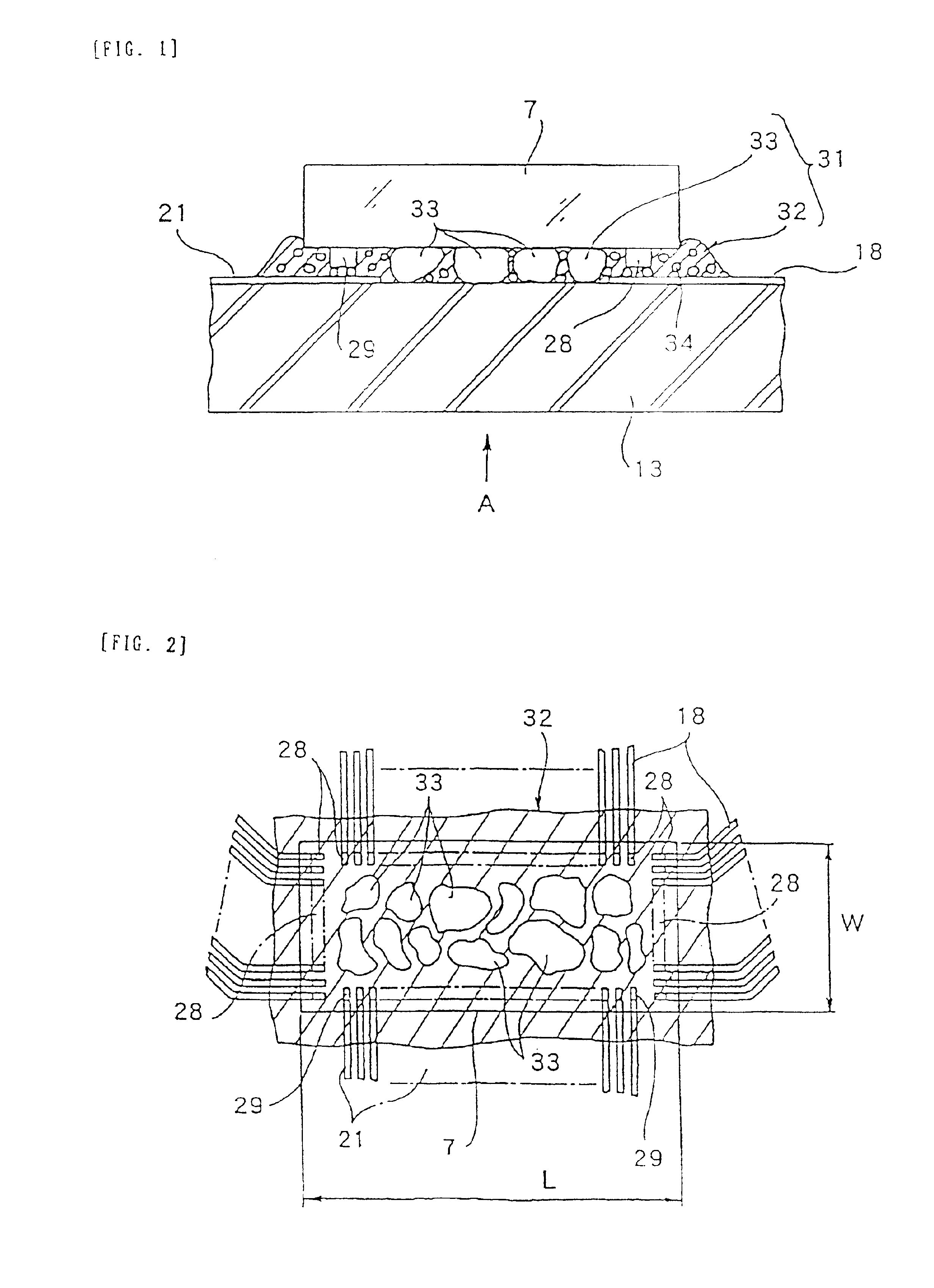
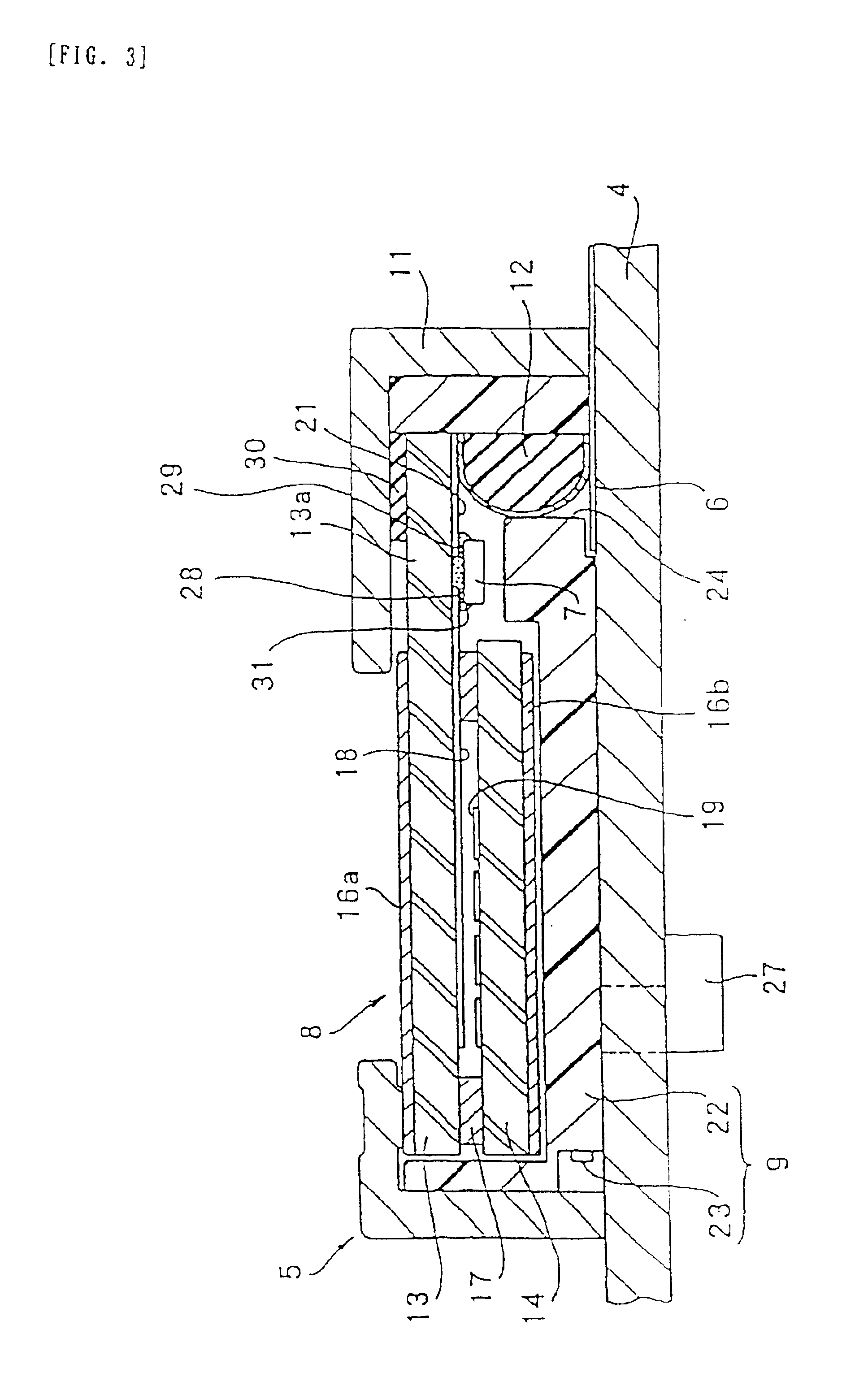
[0008]For the purpose described above, in accordance with the present invention, in a semiconductor device connecting structure for joining a semiconductor device onto a substrate according to this invention, there is a bonding layer in between the substrate and the semiconductor device for adhesion of both of them. The bonding layer contains a bonding material for joining the semiconductor device to the substrate and a space(s) formed in the interior of the bonding material.

[0009]According to this connecting structure, the space(s) is specially made in the bonding material when conducting the adhesion between the semiconductor device and the substrate, and absorb the deformation of the semiconductor device and others, changing freely in shape in response to the deformation of the substrate or the semiconductor device. In consequence, even in the case of the deformation of the semiconductor device or the substrate, it is possible to prevent excessive loads from applying on the elect...


PUM

PropertyMeasurementUnit
widthaaaaaaaaaa
sizeaaaaaaaaaa
sizeaaaaaaaaaa

Abstract

A semiconductor device connecting structure for connecting a semiconductor IC 7 onto a substrate 13. A bonding layer 31 is placed between the substrate 13 and the semiconductor IC 7 to accomplish adhesion therein. This bonding layer includes an ACF 32 as a bonding material for joining said semiconductor IC 7 onto said substrate 13 and a space 33 formed within the ACF 32. Even if the IC 7 deforms due to heat or the like, the deformation is absorbed by the space a 33, whereupon the connecting conditions of bumps 28, 29 can not be unstable.

Description

TECHNICAL FIELD[0001]The present invention relates to a semiconductor device connecting structure for connecting a semiconductor device onto a substrate (or board), a liquid crystal display unit based upon the semiconductor device connecting structure, and an electronic apparatus using-the liquid crystal display unit.BACKGROUND ART[0002]In recent years, liquid crystal display units for displaying visible information have come into widespread use for electronic equipment such as navigation systems, televisions, palm-top computers, electronic organizers and portable telephones. In general, these liquid crystal display units are constructed such that a liquid crystal driving IC, i.e., a semiconductor device, is connected to a liquid crystal panel and incidental parts such as a back light and a casing are mounted on the liquid crystal panel. This liquid crystal panel is commonly made in a manner that a liquid crystal is put in between at least two substrates for the liquid crystal, and ...

Claims


Application Information

Patent Timeline
Patent Type & Authority Patents(United States)
IPC IPC(8): H01L21/56H01L21/02H01L21/60G02F1/13G02F1/136H01L21/52G02F1/1343
CPCH01L21/563H01L24/28H01L24/31H01L24/83G02F1/13452H01L2224/16225H01L2224/73203H01L2224/8319H01L2224/838H01L2924/01004H01L2924/01015H01L2924/01027H01L2924/01033H01L2924/01049H01L2924/0105H01L2924/01074H01L2924/01078H01L2924/01082H01L2924/0781H01L2924/14H01L2924/3025H01L2224/2919H01L2924/01006H01L2924/0665H01L2924/00H01L2924/12041H01L2224/8385
Inventor UCHIYAMA, KENJI
Owner TCL CHINA STAR OPTOELECTRONICS TECH CO LTD
Why Eureka
Try Eureka