DLL circuit

Inactive Publication Date: 2005-09-06
SK HYNIX INC
13 Cites 9 Cited by

AI-Extracted Technical Summary

Problems solved by technology

However, as shown in FIG. 8, the conventional delay circuit causes no problem in a case in which the delay time T2 in the replica delay unit is shorter than the period TCK of the ...

Benefits of technology

[0040]Accordingly, the present invention has been made to solve the above-mentioned problems occurring in the prior art, and an object of the present invention i...

Abstract

A DLL circuit synchronizes an external input clock applied from an outside of a system with an internal input clock used inside the system using a divider unit. The DLL circuit includes a detection unit for detecting whether a pulse width of the external input clock is narrower than a reference set value. The divider unit outputs a first divided signal when it is detected that the pulse width of the external input clock is wider than the reference set value, and outputs a second divided signal when it is detected that the pulse width of the external input clock is shorter than the reference set value. The DLL circuit can normally operate even when the period of the external input clock is short.

Application Domain

Pulse automatic controlDuration/width modulated pulse demodulation +2

Technology Topic

Clock synchronizationFrequency divider

Image

  • DLL circuit
  • DLL circuit
  • DLL circuit

Examples

  • Experimental program(1)

Example

[0062]Hereinafter, preferred embodiments of the present invention will be described with reference to the accompanying drawings. In the following description and drawings, the same reference numerals are used to designate the same or similar components, and so repetition of the description on the same or similar components will be omitted. Also, in the description, the expression of “—the period of the clock signal is short or small—” means that the pulse width of the clock signal is narrow, and “—the period of the clock signal is long—” means that the pulse width of the clock signal is wide.
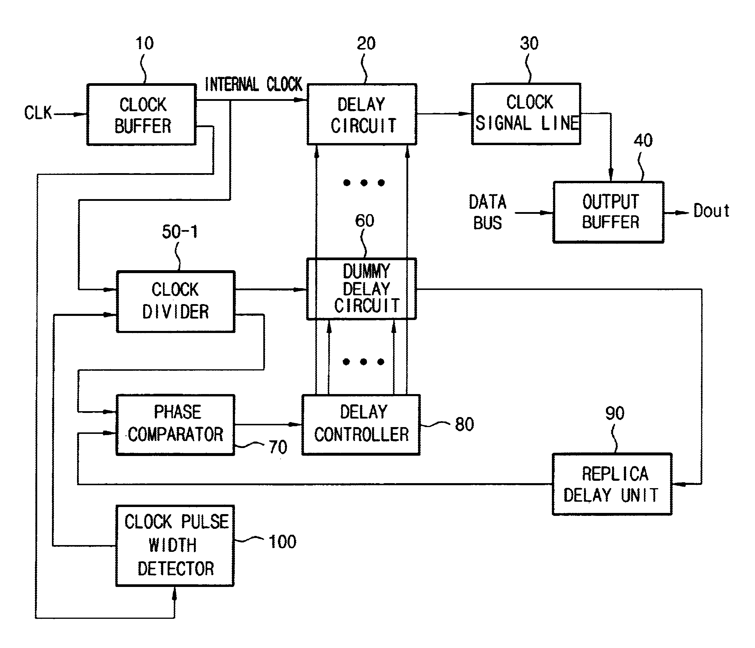
[0063]FIG. 9 is a block diagram of a DLL circuit according to the present invention.
[0064]As shown in FIG. 9, the DLL circuit according to the present invention includes a clock buffer 10 for receiving an external clock signal, a delay circuit 20 for receiving an output signal of the clock buffer 10, a clock divider 50-1 for dividing the output signal of the clock buffer 10, a dummy delay circuit 60 for delaying an output signal of the clock divider 50-1 for a predetermined time, a replica delay unit 90 for delaying an output signal of the dummy delay circuit 60, a phase comparator 70 for comparing a phase of an output signal of the replica delay unit 90 with a phase of the output signal of the clock divider 50-1, a delay controller 80 for receiving an output signal of the phase comparator 70 and controlling delay operations of the delay circuit 20 and the dummy delay circuit 60, a clock signal line 30 for receiving an output signal of the delay circuit 20 and controlling a data output of an output buffer 40, and a clock pulse width detector 100 for receiving the output signal of the clock buffer 10 and detecting a pulse width of the clock signal.
[0065]The DLL circuit according to the present invention has many parts similar to those of the conventional DLL circuit, but, as distinct from the conventional DLL circuit, is provided with the clock pulse width detector 100. Also, since the clock divider 50-1 according to the present invention receives an output signal of the clock pulse width detector 100, its construction is different from that of the conventional DLL circuit.
[0066]Hereinafter, the construction and function of the clock pulse width detector 100 and the clock divider 50-1 will first be explained, and then the whole operation of the present invention will be explained.
[0067]FIG. 11 illustrates an example of the clock pulse width detector used in the DLL circuit according to the present invention, and FIG. 12 is a timing diagram of the clock pulse width detector illustrated in FIG. 11.
[0068]As illustrated in FIGS. 11 and 12, the clock pulse width detector receives a clock signal, delays the clock signal several times and then selectively outputs a logical low or high-level signal through a latch circuit.
[0069]In operation, if the clock signal is inputted, a low-level pulse signal ‘a’ is generated after a predetermined time delay. If the high-level pulse width of the clock signal exceeds the predetermined delay time (i.e., exceeds a delay time through a delay 2), a low-level pulse signal is generated at a node b, and if the high-level pulse width of the clock signal is less than the predetermined delay time (i.e., below the delay time through the delay 2), the node b is kept in a high level.
[0070]In summary, if the pulse width of the input clock signal is longer than the predetermined delay time, the node b outputs the low-level pulse signal, and if the pulse width of the clock signal is shorter than the predetermined delay time, the node b is kept in the high level.
[0071]As shown in FIGS. 11 and 12, if the pulse width is longer than the predetermined delay time, the clock pulse width detector outputs a low-level signal, while if the pulse width is narrower than the predetermined delay time, the clock pulse width detector outputs a high-level signal. In the embodiment of the present invention, the external input clock and the output signal of the clock buffer have the same period and the same duty rate, and the duty rate is 50%. Also, the clock pulse width detector uses the high-level pulse width of the output signal of the clock buffer in order to detect whether the period of the output signal of the clock buffer exceeds the predetermined delay time.
[0072]FIG. 10 illustrates an example of a clock divider used in the DLL circuit according to the present invention.
[0073]As illustrated in FIG. 10, the clock divider 50-1 includes a plurality of dividers 51, 52, 54 and 55. A multiplexer 53 is a switching means which selects one among the output signals of the two dividers 51 and 52.
[0074]Under the control of the multiplexer 53, the dividers are connected in the order of 51-52-54-55 or in the order of 51-54-55. An output signal of the clock pulse width detector is used as the control signal Short_tck of the multiplexer 53. If the pulse width (or period) of the clock signal CLK applied to the clock divider is wide, the output signal of the divider 51 is selected through the multiplexer 53, and if the pulse width (or period) of the clock signal CLK applied to the clock divider is narrow, the output signal of the divider 52 is selected through the multiplexer 53.
[0075]In FIG. 10, the divider51 outputs a clock signal CLK_1 obtained by dividing the frequency of the clock signal CLK into ½. The divider 52 outputs a clock signal aa obtained by dividing the frequency of the clock signal CLK_1 into ½. Thus, the frequency of the output signal aa of the divider 52 is ¼ of the frequency of the clock signal CLK.
[0076]The signal inputted to the divider 54 is the output signal of the divider 51 or the output signal of the divider 52, and the signal inputted to the divider 55 is an output signal of the divider 54.
[0077]Accordingly, the frequency of the signal outputted through the clock divider is ⅛ or 1/16 of the frequency of the clock signal CLK inputted to the clock divider.
[0078]The duty rates of the output signals of the dividers 5, 52, 54 and 55 are not identical, but it is possible to modify the duty rates if needed.
[0079]As described above, if the frequency of the external input clock is lower than the reference set value, the clock divider outputs the first divided signal (i.e., in FIG. 11, 1/16-divided signal), and if the frequency of the external input clock is higher than the reference set value, the clock divider outputs the second divided signal (i.e., in FIG. 11, ⅛-divided signal).
[0080]FIG. 13 is a timing diagram of the DLL circuit according to the present invention in the case where the period of the input clock signal is long.
[0081]In FIG. 13, TCK denotes the period of the clock signal, and T1 denotes a delay time occurring as the externally inputted clock passes through the clock buffer.
[0082]T2 denotes a delay time occurring from the input of the external clock to the output of the data, and is the same as the delay time of the delay unit 90.
[0083]Td denotes a delay time which should be adjusted in the delay circuit 20 by the delay controller 80.
[0084]CLK_DLL denotes the output signal of the clock signal line 30 which controls the data output buffer 40, and dout denotes data which is outputted from the data output buffer 40.
[0085]CLK_3 and CLK_3b denote final output signals of the clock divider, and CLK_3delay denotes the output signal of the replica delay unit. If the period of the input clock signal is long, the clock divider uses only the dividers 51, 54 and 55, and thus the frequency of the final output signals becomes ⅛ of the frequency of the clock signal inputted to the clock divider. For reference, in FIG. 13, the expression of “if the period of the input clock signal is long’ means that the period of the clock signal TCK is wider than T2.
[0086]FIG. 14 is a timing diagram of the DLL circuit according to the present invention in the case where the period of the input clock signal is short. In this case, the period TCK of the external input clock is shorter than the time T2_1 taken from the input of the external clock to the output of the data. In this case, the clock pulse width detector 100 detects that the period of the input clock is short, and outputs a high-level signal.
[0087]If the period of the input clock signal is short, the clock divider uses the dividers 51, 52, 54 and 55, and thus the frequency of the final output signal is 1/16 of the frequency of the clock signal inputted to the clock divider. Accordingly, the frequency of the final output signals CLK_3 and CLK_3b of the clock divider becomes 1/16 of the frequency of the external input clock. In this case, the high-level pulse width of the final output signals CLK_3 and CLK_3b is 2TCK as shown in FIG. 14. Accordingly, even if the period of the external input clock is short, the DLL circuit can normally operate.
[0088]As described above, according to the present invention, since the period of the clock inputted to the clock divider is lengthened four times, and then the clock is divided through the dividers 54 and 55, it is possible for the phase comparator 70 to perform a phase comparison and for the delay controller 80 to control the dummy delay circuit 60 and the delay circuit 20, and thus the DLL circuit can normally operate even if the period of the external input clock is short.
[0089]Although preferred embodiments of the present invention have been described for illustrative purposes, those skilled in the art will appreciate that various modifications, additions and substitutions are possible, without departing from the scope and spirit of the invention as disclosed in the accompanying claims.

PUM

no PUM

Description & Claims & Application Information

We can also present the details of the Description, Claims and Application information to help users get a comprehensive understanding of the technical details of the patent, such as background art, summary of invention, brief description of drawings, description of embodiments, and other original content. On the other hand, users can also determine the specific scope of protection of the technology through the list of claims; as well as understand the changes in the life cycle of the technology with the presentation of the patent timeline. Login to view more.

Similar technology patents

Pressing explosion type dual-inner tube tire

InactiveCN104985989AImprove securityNormal operationWith separate inflatable insertsSpare tireEngineering
Owner:NINGBO UNIVERSITY OF TECHNOLOGY

Liquid level detection device

ActiveUS20200278236A1Normal operationMachines/enginesLubrication indication devicesViscous liquidStructural engineering
Owner:HOKWANG IND

Low profile auxiliary lubrication system

ActiveUS20200340574A1Normal operationAbnormal operationEngine fuctionsGear lubrication/coolingLubricationVariator
Owner:LOCKHEED MARTIN CORP

Classification and recommendation of technical efficacy words

Why Eureka
Try Eureka