Semiconductor light emitting device

a technology of semiconductors and light emitting devices, which is applied in the direction of point-like light sources, lighting and heating apparatus, instruments, etc., can solve the problems of reduced efficiency of led, limited use of light emitting diodes (leds) that are currently used, and increased heat generation of leds

Inactive Publication Date: 2005-09-06
GELCORE LLC (US)
View PDF39 Cites 98 Cited by
  • Summary
  • Abstract
  • Description
  • Claims
  • Application Information

AI Technical Summary

Benefits of technology

[0007]Therefore, a need has arisen for an LED having a combination of features that enable it to generate more light than is possible with standard die, and to operate reliably in higher temperature thermal environments (exceeding 85° C.) and at higher drive currents (exceeding 50 mA) while using reflow solderable LED packages.

Problems solved by technology

Light emitting diodes (LEDs) that are currently used have limitations.
But, at higher drive currents, an LED generates a greater amount of heat.
And, as the temperature of the LED die increases, the LED becomes less efficient and thus, its brightness is reduced.
As an LED die experiences increasing temperatures during operation, not only can its efficiency be reduced, but it can also create reliability problems within the LED structure.
Further, increased die temperature may also lead to a wavelength shift in the LED.
But, use of through-hole leaded packages in circuit board assemblies requires the use of a costly and difficult to control wave solder process.
The drive current of an LED is also limited by the mounting of the semiconductor die within the package.
The wire bond and epoxy, however, are also susceptible to deterioration due to the effects of heat.
That is, as the epoxy heats and cools, the epoxy expands, causing stress in the wire.
Eventually, the LED may fail due to stress and a break in the wire bond.
While these configurations improve the reliability of the anode and cathode to die connections compared to use of a wire bond, they have not heretofore been used in high current (above 50 mA) LED devices.
These and other drawbacks exist with conventional LEDs.

Method used


Image

  • Semiconductor light emitting device
  • Semiconductor light emitting device
  • Semiconductor light emitting device

Examples


Embodiment Construction

[0019]While the foregoing description includes many details and specifics, it is to be understood that these have been included for purposes of explanation only, and are not to be interpreted as limitations of the present invention. Many modifications to the embodiments described can be made without departing from the spirit and scope of the invention, as is intended to be encompassed by the following claims and their legal equivalents.

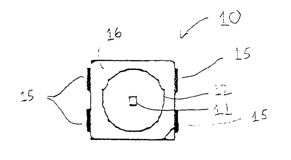
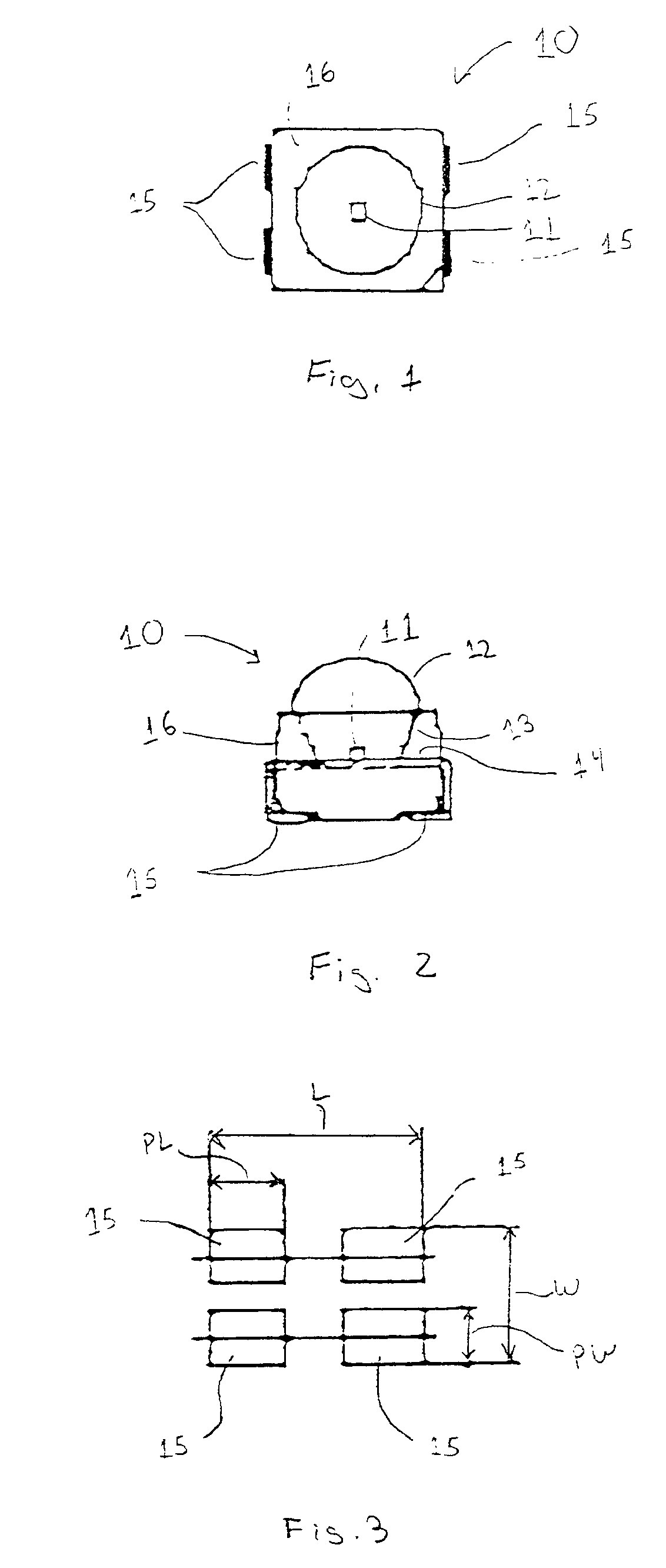
[0020]The LED of the present invention includes a unique combination of features that enable the LED to produce a high-brightness predetermined radiation pattern. The combination of features enable the LED to function reliably at a higher drive current at a given ambient temperature, and therefore emit light of increased brightness, and to have a particular, e.g., symmetrical, radiation pattern.

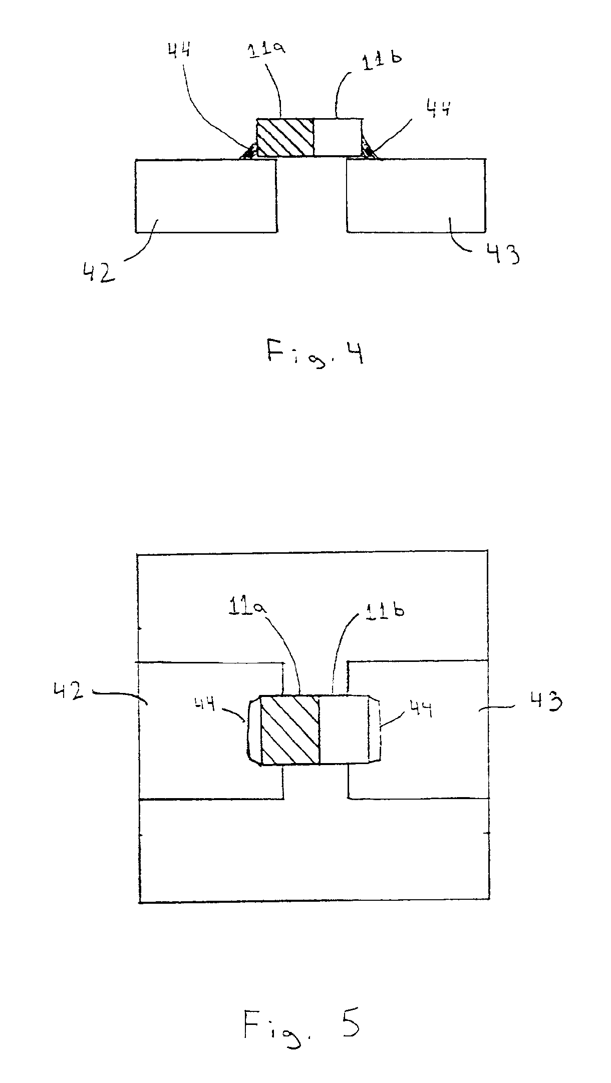
[0021]An LED according to one embodiment of the present invention will now be explained in conjunction with FIGS. 1-9. FIGS. 1 and 2 depict top and cross-secti...


PUM


Abstract

A light emitting diode (LED) including a combination of features that enable the LED to produce a high-brightness predetermined radiation pattern. The combination of features enable the LED to function cooler and more reliably at a higher drive currents and elevated ambient temperatures, and therefore emit light of increased brightness, without overheating, and to have a particular radiation pattern. In particular, a surface mount that is capable of operating at high drive currents and high ambient temperatures is disclosed. The LED comprises a surface mount package having a metal lead frame having mass sufficient to provide low thermal resistance, at least one anode contact pad and at least one cathode contact pad. The LED also includes a reflector positioned within the package, a semiconductor die and an optional focusing dome. The semiconductor die comprises a transparent substrate and a semiconductor component and is positioned within the package so that the semiconductor component and the substrate are arranged side-by-side over the reflector (flop-chip). Alternatively, the die is positioned within the package so that the substrate is on top of the semiconductor component (flip-chip). The optional focusing dome is operative to refract light emitted from the semiconductor die and light reflected from the reflector to create a predetermined radiation pattern.

Description

BACKGROUND OF THE INVENTION[0001]This invention relates to a semiconductor light emitting device having increased current capacity and increased brightness. In particular, this invention relates to a light emitting diode (LED) having a configuration that includes a highly thermally conductive surface mount package that enables the use of higher drives currents and thus produces increased brightness.[0002]Light emitting diodes (LEDs) that are currently used have limitations. For example, at relatively low drive currents, the amount of flux an LED produces is directly related to its drive current. For most applications, it is desirable to drive LEDs at as high a current as possible in order to maximize the brightness of their emission. But, at higher drive currents, an LED generates a greater amount of heat. And, as the temperature of the LED die increases, the LED becomes less efficient and thus, its brightness is reduced. As an LED die experiences increasing temperatures during oper...

Claims


Application Information

Patent Timeline
Patent Type & Authority Patents(United States)
IPC IPC(8): H01L33/00H01L33/48H01L33/58H01L33/62H01L33/64
CPCH01L33/486H01L33/58H01L33/62H01L33/64H01L2924/0002H01L2924/00
Inventor STALIONS, DRAKE CHARLES
Owner GELCORE LLC (US)
Why Eureka
Try Eureka