Data processing system and data processing method

a data processing system and data processing technology, applied in the direction of circuit optical details, printed circuit non-printed electric components association, instruments, etc., can solve the problems of small progress in reducing the ratio of logic area to total chip area, ic chip has a relatively small ratio of circuit area to total chip area, ic chip has an extremely small ratio of logic area to total area, etc., to achieve the effect of reducing the size of ic chip

Inactive Publication Date: 2005-09-13
GLOBALFOUNDRIES US INC
View PDF16 Cites 75 Cited by
  • Summary
  • Abstract
  • Description
  • Claims
  • Application Information

AI Technical Summary

Benefits of technology

[0006]It is an object of the present invention to provide a data processing system and a data processing method having reduced IC chip sizes.

Problems solved by technology

However, little progress has been made in a technique for reducing intervals between I / O (Input / Output) pads on the chip.
Even if a logic region occupies an extremely small portion of the entire chip, the die size cannot be reduced because of the need to maintain a predetermined number of I / O's, leading to an IC chip having a relatively small ratio of circuit area to total chip area.
However, the technique like the crossbar switch system results in forming too many pins, also leading to an IC chip having an extremely small ratio of logic area to total area.
The IC chip with the wireless communications capability incorporated in the IC card makes communications not with an IC chip that can be connected via wire, but with an access control system or a charging system, which inherently has a difficulty in establishing a wired connection.

Method used


Image

  • Data processing system and data processing method
  • Data processing system and data processing method
  • Data processing system and data processing method

Examples


Embodiment Construction

[0047]The best mode of the present invention will now be described with reference to the accompanying drawings.

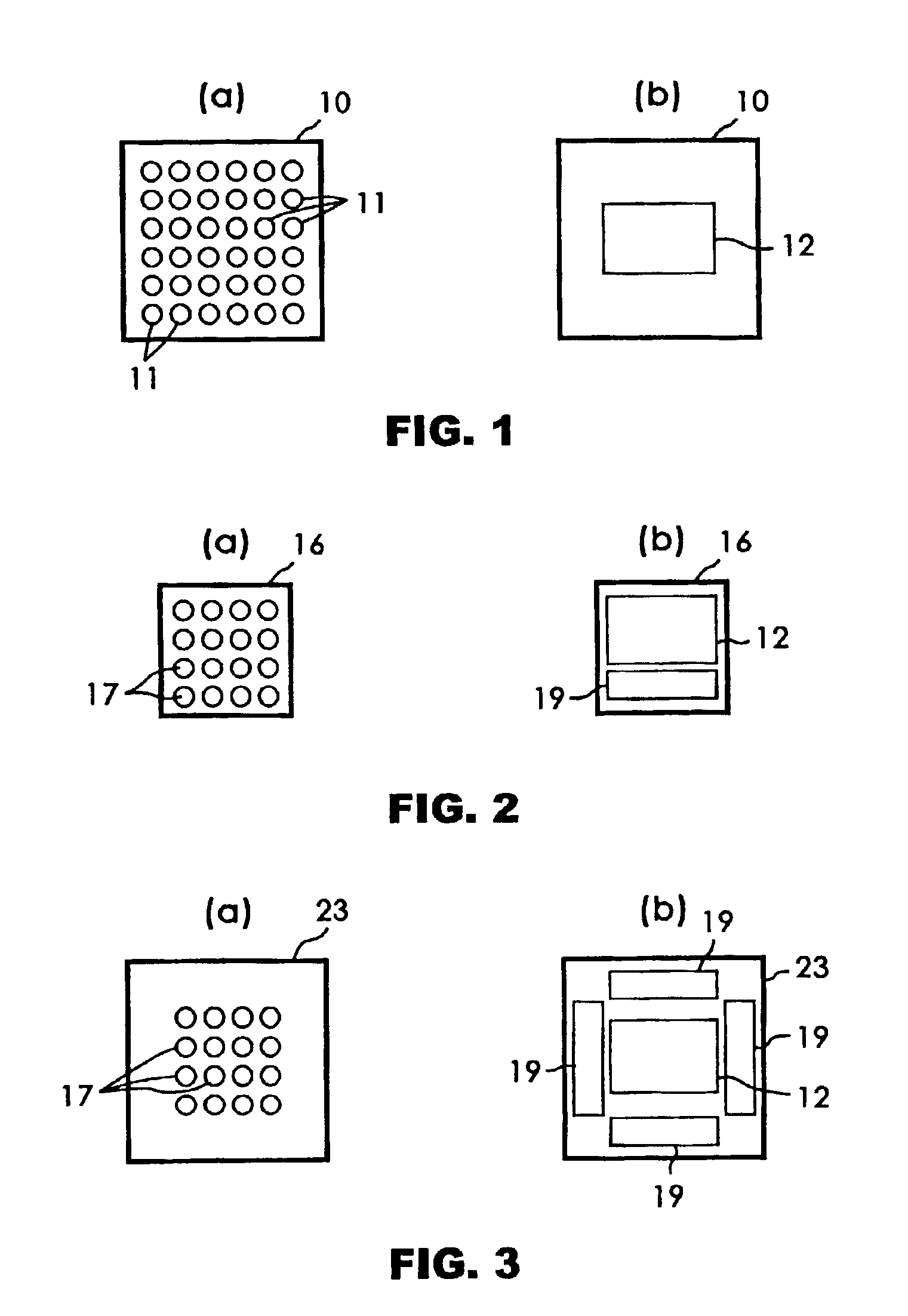
[0048]FIGS. 1(a) and 1(b) illustrate an IC chip 10 having pads including I / O pads. IC chips 10, 16 and 23 shown in FIGS. 1(a), 1(b), 2(a), 2(b), 3(a) and 3(b), respectively, may be mounted on a substrate by direct mounting via solder bumps, or packaging with mold resin, or fixing to a module substrate. FIG. 1(a) shows a distribution of bonding pads 11 on IC chip 10, and FIG. 1(b) shows an area ratio of IC chip 10 and a logic section 12. Bonding pads 11 include pads connected to a VDD (power supply) and a GND (ground) in addition to the S / O pads. Bonding pads 11 are arranged in a grid form. Although the area of logic section 12 is small, the need to maintain all bonding pads 11 including the I / O pads makes it difficult to reduce the size of IC chip 10. Accordingly, an area ratio of logic section 12 to the surface area of IC chip 10 is relatively small.

[0049]FIGS. 2(a) and 2(...


PUM


Abstract

An IC chip is provided with a wireless unit for inputting and outputting data by wireless communication, in addition to a logic section, so that the IC chip no longer needs I/O pads, leaving only power supply and ground pads. IC chips can input and output data with one another by wireless communications, which makes it possible to significantly improve the spacing relationships of various chips on a singular or even plurality of substrates.

Description

FIELD OF THE INVENTION[0001]The present invention relates to a data processing system and a data processing method implemented in a computer or the like.BACKGROUND OF THE INVENTION[0002]Advancements of submicron technologies in semiconductor manufacturing make it possible to form large-scale logic in a single IC chip. However, little progress has been made in a technique for reducing intervals between I / O (Input / Output) pads on the chip. This means that the size of the chip is determined by the number of I / O's rather than the number of logics. Even if a logic region occupies an extremely small portion of the entire chip, the die size cannot be reduced because of the need to maintain a predetermined number of I / O's, leading to an IC chip having a relatively small ratio of circuit area to total chip area.[0003]On the other hand, the design concept of sharing a bus by various I / O's and devices has reached the limit in speeding up the system, and an attempt is being made to solve a prob...

Claims


Application Information

Patent Timeline
Patent Type & Authority Patents(United States)
IPC IPC(8): H05K1/02H05K1/18H01L21/822G06K19/07H01L27/04H01Q1/38
CPCH05K1/0274H05K1/181H05K2201/10734H01L2224/16225H01L2224/73204H01L2924/15311H01L2223/6677
Inventor NOZAWA, TOHRUKATO, YOSHIHARU
Owner GLOBALFOUNDRIES US INC
Why Eureka
Try Eureka