Chip resistor

a chip and resistor technology, applied in the direction of resistor details, resistors adapted for terminal application, resistive material coating, etc., can solve the problems of inability to solve the problem, inability to use ni—cr or ni—ti, and loss of thin films made of ni—cr

Inactive Publication Date: 2005-09-13
ROHM CO LTD
View PDF2 Cites 40 Cited by
  • Summary
  • Abstract
  • Description
  • Claims
  • Application Information

AI Technical Summary

Problems solved by technology

Such thin-film resistors, however, have a problem in that if, for example, human sweat, seawater, etc. are adhered thereto, there occurs chemical reaction between NaCl contained in human sweat, seawater, etc. and Ni—Cr due to presence of moisture, thereby causing the thin films made of Ni—Cr to be lost.
In such a case, as for the resistance, a constituent material other than Ni—Cr, not reacting with NaCl etc., can be selected, however, for the side electrodes, use of Ni—Cr or Ni—Ti is unavoidable in view of such problems as resistivity and oxidation, so that it has been impossible to resolve the problem described above.

Method used


Image

  • Chip resistor
  • Chip resistor
  • Chip resistor

Examples


first embodiment

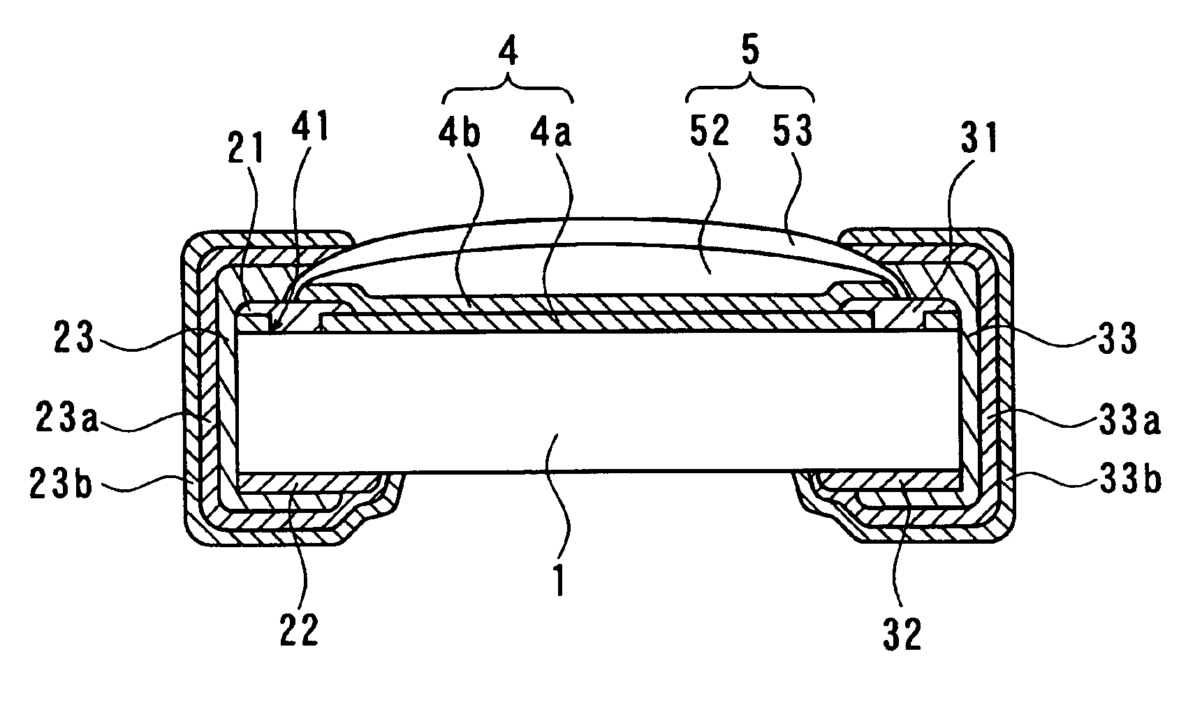
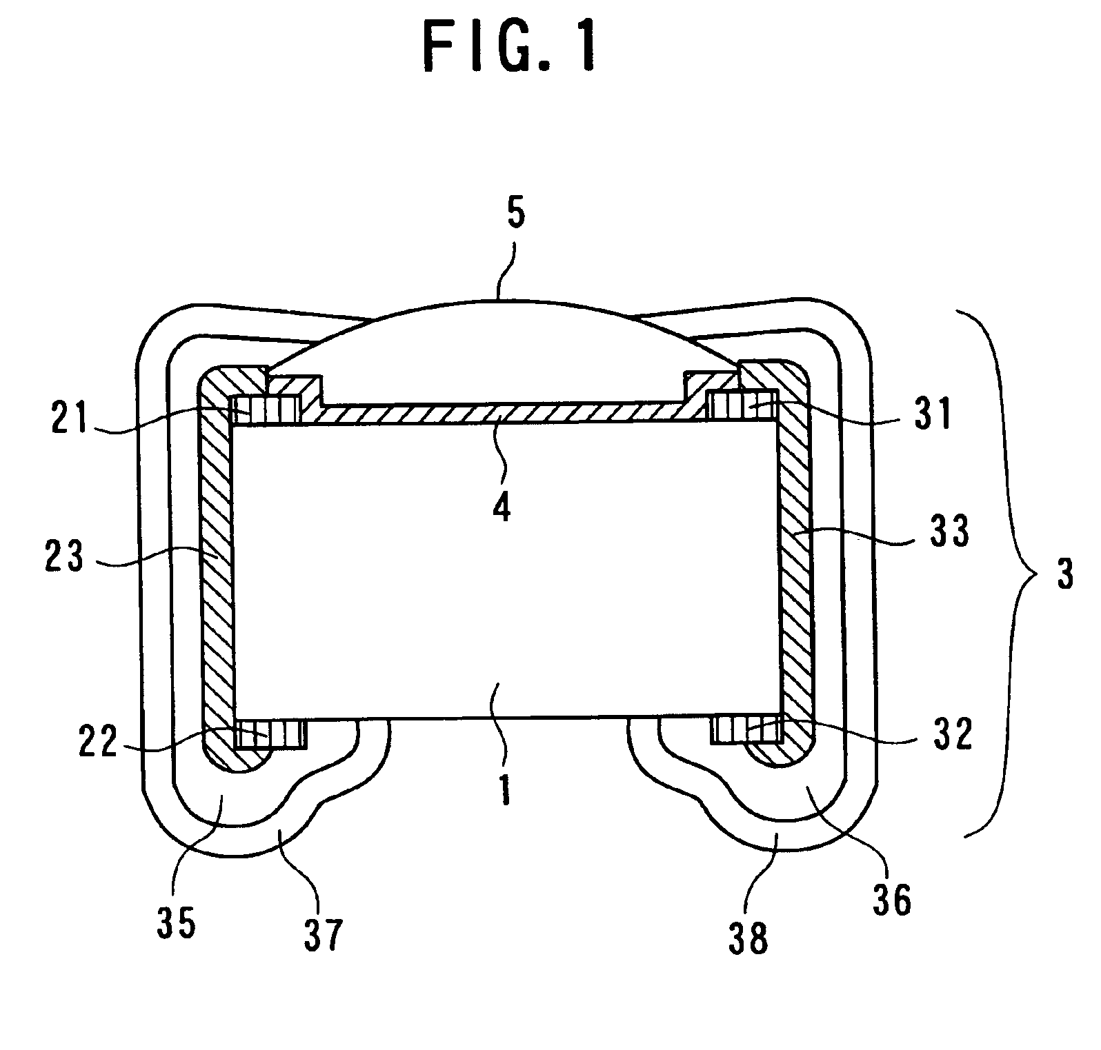
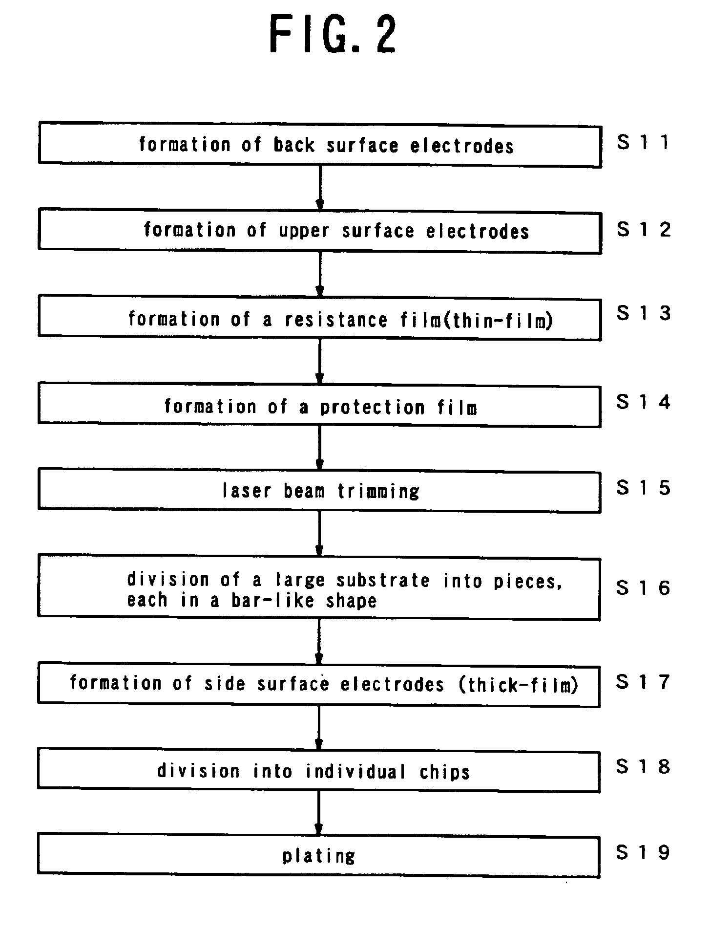
[0023]As schematically shown in FIG. 1, with a chip resistor according to a first embodiment, there are provided upper surface electrodes 21, 31, formed of a thick-film, and back surface electrodes 22, 32, formed of a thick-film, at opposite ends of the top surface and back surface of an insulating substrate 1 made of, for example, alumina, and rectangular in plan view, respectively, and further, the upper surface electrodes and the back surface and electrodes are electrically bonded with each other through the intermediary of thick-film electrodes such as side surface electrodes 23, 33, respectively. Further, a thin-film resistance 4 is formed on an exposed part between the opposite ends of the top surface of the insulating substrate 1, and on respective portions of the upper surface electrodes, and in addition, a protection film 5 is provided on the top surface of the resistance 4.

[0024]In the figure, for the substrate 1, use is made of, for example, alumina, sapphire, or Si wafer...

second embodiment

[0033]FIG. 3 shows a second embodiment of a chip resistor according to the invention.

[0034]The second embodiment shown in FIG. 3 is the same as the first embodiment except that thick-film upper surface electrodes 21, 31 are divided into first upper surface electrodes 21A, 31A and thick-film auxiliary electrodes 21B, 31B as second upper surface electrodes, and a resistance 4 formed of a thin film is sandwiched between the first upper surface electrodes 21A, 31A, formed of the thick film, and the second upper surface electrodes 21B, 31B, formed of the thick film, thereby making up a sandwich structure.

[0035]Further, a method of fabricating the chip resistor according to the second embodiment is the same as the method of fabricating the chip resistor according to the first embodiment except that after the thin-film resistance 4 made of Ta—N, Ta—Cr, etc. are formed as in the method of fabricating the chip resistor according to the first embodiment, the thick-film auxiliary electrodes 21...

third embodiment

[0037]FIG. 4 shows a third embodiment of a chip resistor according to the invention, wherein in the case of adopting a composite body made up of a thin-film and a thick-film, and in particular, in the case of adopting a construction in which a thick-film is formed on top of a thin-film, means for enhancing tackiness between the thin-film and the thick-film formed thereon are provided.

[0038]That is, with the third embodiment shown in FIG. 4, upper surface electrodes 21, 31 are divided into first upper surface electrodes 21a, 31a and second upper surface electrodes 21b, 31b and a resistance 4 formed of the thin-film is sandwiched between the first upper surface electrodes 21a, 31a, formed of the thick film, and the second upper surface electrodes 21b, 31b, formed of the thick film as with the second embodiment, however, in this case, a through-hole 41 is provided in part of the resistance 4, on top of respective portions of the first upper surface electrodes 21a, 31a, thereby keeping ...


PUM


Abstract

Resistance or side electrodes of a chip resistor is prevented from being lost due to chemical reaction with NaCl contained in human sweat and so on when human sweat, seawater, etc. are adhered thereto. The chip resistor comprises an insulating substrate, thick-film upper surface electrodes formed at opposite ends of the top surface of the insulating substrate, a thin-film resistance made of a constituent material not reacting with NaCl, and formed so as to be extended over the upper surface of the insulating substrate and respective portions of the upper surface of the thick-film upper surface electrodes, thick-film back surface electrodes formed at spots on the back surface of the insulating substrate, corresponding to the thick-film upper surface electrodes, respectively, and thick-film side surface electrodes connecting the thick-film back surface electrodes with respective portions of the thick-film upper surface electrodes, exposed out of the thin-film resistance, respectively.

Description

BACKGROUND OF THE INVENTION[0001]1. Field of the Invention[0002]The invention relates to a chip resistor comprising a chip type insulating substrate with a thin-film resistance provided thereon. More specifically, the invention is intended to provide a chip resistor provided with a resistance or electrodes that will not be lost upon coming in contact with human sweat or seawater.[0003]2. Description of the Related Art[0004]Conventional chip resistors include a thick-film resistor provided with electrodes and a resistance, formed by printing and firing constituent materials thereof, and a thin-film resistor provided with electrodes and a resistance, formed by sputtering constituent materials thereof. Both are substantially same in construction although they differ from each other in that one is formed of a thick-film while the other is formed of a thin-film, and in respect of vertical relationship between the resistance and upper electrodes. That is, as shown in FIG. 9, at opposite e...

Claims


Application Information

Patent Timeline
Patent Type & Authority Patents(United States)
IPC IPC(8): H01C17/00H01C17/065H01C7/00H01C17/28H01C17/06H01C1/142H01C1/14
CPCH01C1/142H01C7/003H01C17/006H01C17/06513H01C17/281
Inventor TANIMURA, MASANORI
Owner ROHM CO LTD
Why Eureka
Try Eureka