[0006]It is, inter alia, an object of the invention to decrease the power dissipation in the data drivers.
[0008]In a
driver circuit for a matrix display in accordance with a primary aspect of the invention, a bias circuit increases a bias current of the data driver only when an edge of at least one of the data signals occurs or is expected to occur. In this way, the bias current can be selected to be very small if no edge of the
data signal occurs or is expected to occur, and the power dissipation in the data driver will be lowered. If no edge occurs or is expected to occur, the bias current has a low value during the whole select time (also referred to as address time) of a row. If an edge occurs, there are several possibilities of realizing the required
short duration of the data setup time: the bias current has a high value during the whole select time of a row, or, preferably, only during the data setup period. A significant reduction of power dissipation will be reached already if the bias current has a small value during at least part of the period outside the data setup period. The
short duration of the data setup time may be reached also if the bias current has a high value during part of the data setup time only.
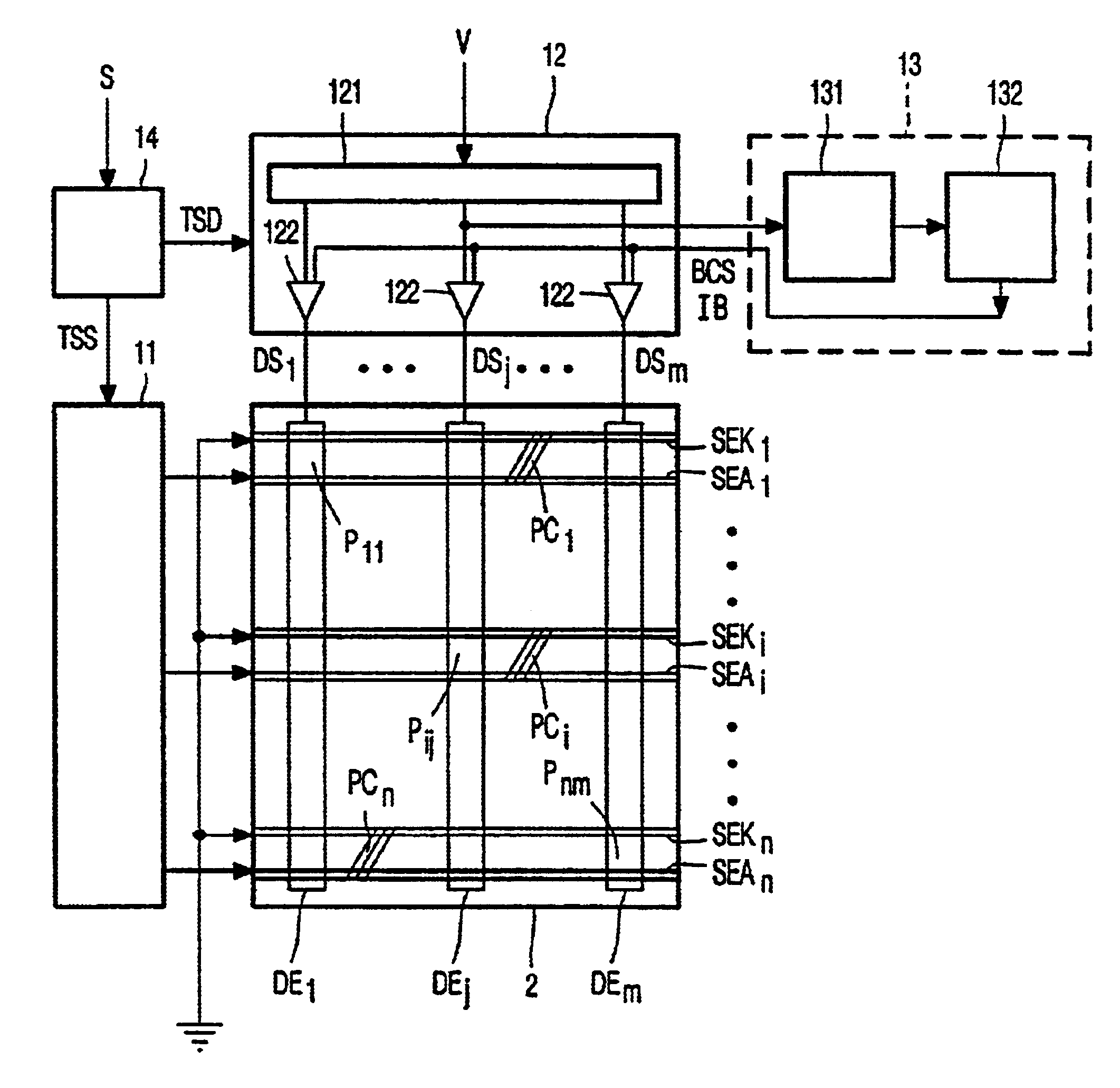
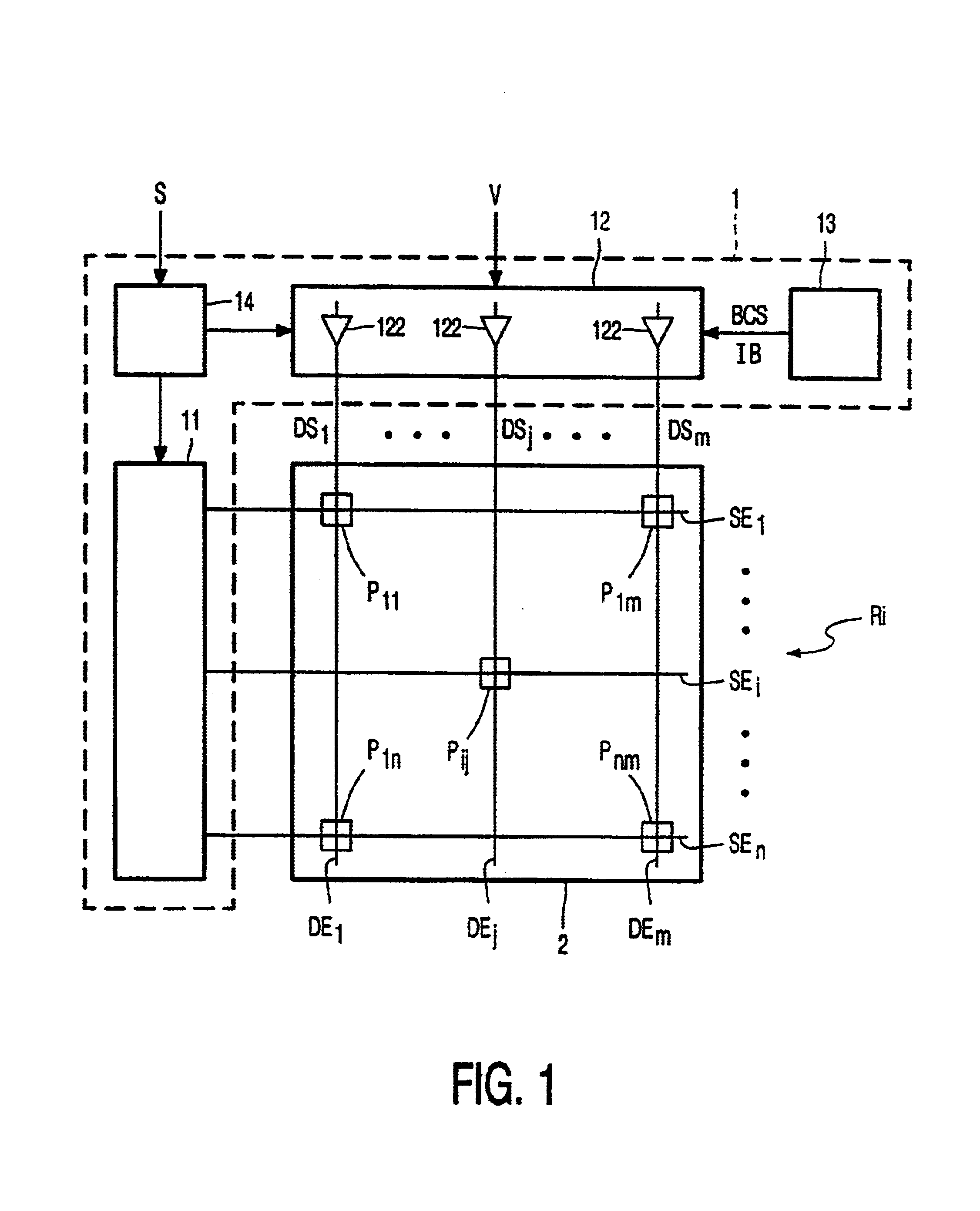
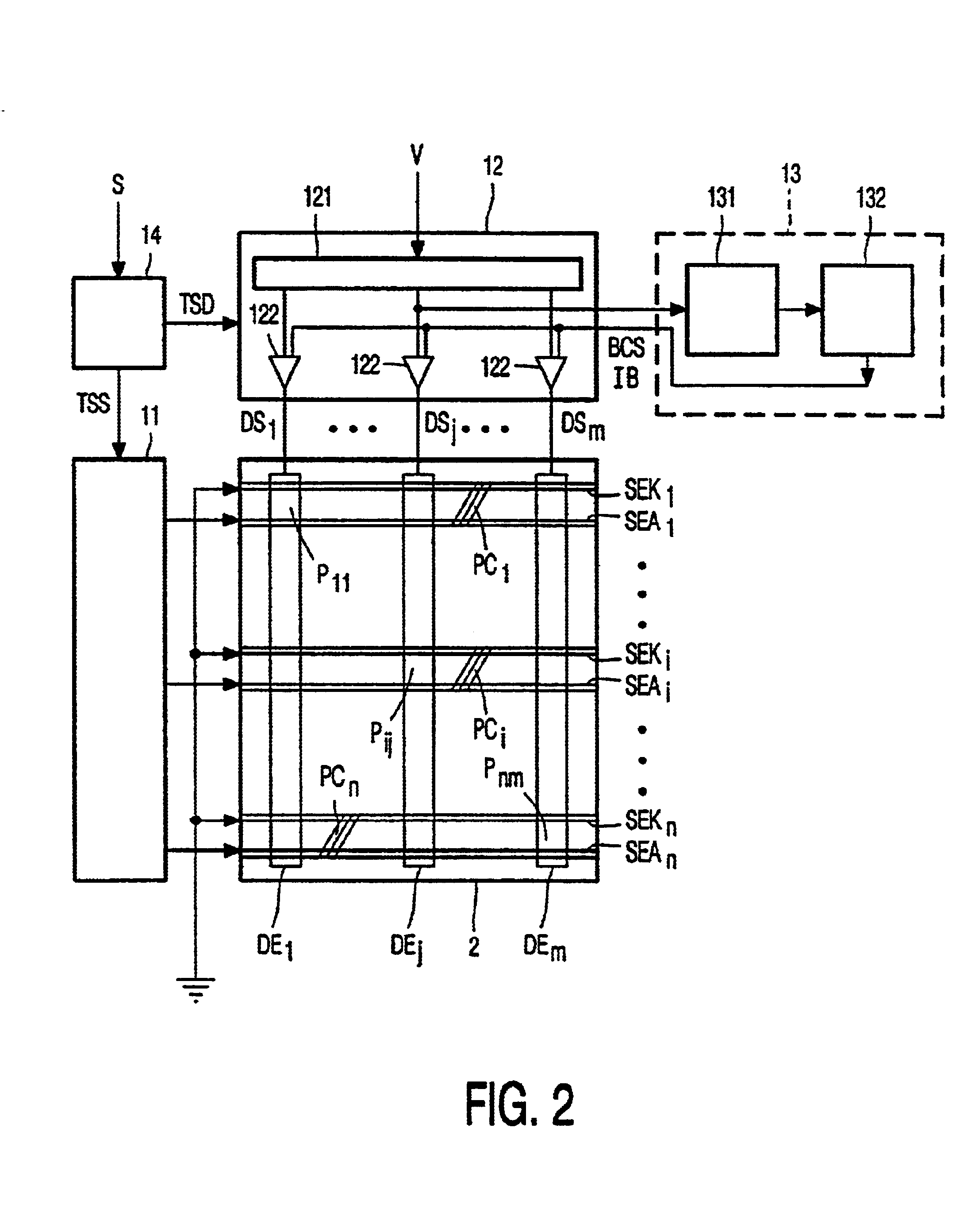
[0010]In another embodiment of the invention, the bias
control signal controls the bias current of all the output stages of the driver circuit. In this way, if a data edge has been detected in a single
data signal associated with one of the data electrodes, all the output stages increase their bias current. Only one
detector is required. A drawback is that it may happen that no data edge occurs in the monitored data
signal, although data edges may occur on unmonitored data electrodes. In a more practical setup, the detection circuit comprises a plurality of detectors, each
detector monitoring one data
signal of a subset of the data signals. If one of the detectors detects a data edge, the bias current of all output amplifiers is increased. In this way, the number of detectors is smaller than the number of data signals or the number of data electrodes, while there is a small chance for usual video signals that no edge occurs on the monitored data electrodes, although a data edge occurs on one of the unmonitored data electrodes. Thus, in a certain row, the bias current will be increased only if at least one data edge has been detected.
[0011]In yet another embodiment of the invention, a detection circuit is associated with each data
signal or data
electrode. The bias current of a certain output stage supplying one of the data signals to the associated one of the data electrodes is increased when the detection circuit associated with this data signal or with this data
electrode detects a data edge in this data signal. This has the
advantage that only the bias current of those output stages at which a data edge has been detected will be increased, which decreases the power dissipation even further.
[0012]In still another embodiment of the invention, a timing
control circuit controls the periods of time during which the bias current is increased. The timing
control circuit controls the instants at which the data signals have to be supplied to the data electrodes after the display elements associated with a select
electrode have been selected. In the preferred situation, in which the data signals are supplied in parallel to the data electrodes, the timing
control circuit knows at which instant the data edges start and is therefore able to increase the bias current of all output stages in relation to this instant. An
advantage of this approach is that
no detection circuits are needed at all. A drawback is that the bias current will be increased during fixed periods of time when a data edge is expected to occur, irrespective of whether the data edge occurs or not. In the situation in which the data signals would be serially supplied to the data electrodes, the timing control circuit again knows when a data edge may occur on which data electrode. Now, the timing control circuit successively increases the bias current of the output stage expected to supply a data edge. In both situations, it is advantageous to start the increase of the bias current shortly before the instant when the data edge may occur, such that the output
amplifier immediately responds with full speed to the data edge when received.

