Integrated circuit redistribution package

a technology of integrated circuits and redistribution packages, which is applied in the direction of printed circuits, semiconductor devices, semiconductor/solid-state device details, etc., can solve the problems of cavity noise and prior art coplanar redistribution packages that often suffer from signal noise, so as to reduce the likelihood of noise coupling in the package, reduce pitch, and increase pitch

Inactive Publication Date: 2005-09-20
GLOBALFOUNDRIES INC
View PDF17 Cites 8 Cited by
  • Summary
  • Abstract
  • Description
  • Claims
  • Application Information

AI Technical Summary

Benefits of technology

[0008]It is therefore a principal object and advantage of the present invention to provide a redistribution package that permits connection of a chip to a printed circuit board without generating cavity noise.
[0009]It is an additional object and advantage of the present invention to provide a redistribution package that does not utilize signal vias.
[0010]It is a further object and advantage of the present invention to provide a redistribution package that diminishes the likelihood of noise coupling in the package.
[0011]Other objects and advantages of the present invention will in part be obvious, and in part appear hereinafter.SUMMARY OF THE INVENTION
[0012]In accordance with the foregoing objects and advantages, the present invention provides a redistribution package having an upper surface that includes contacts with reduced pitch that corresponds, for example, to that of a Controlled Collapse Chip Connection (“C4”) structure formed on a chip, and a lower surface having contacts with increased pitch that correspond, for example, to a printed circuit board employing ball grid array (“BGA”) pads. A series of power, signal and ground conductors extend through the body of the redistribution package and interconnect the circuit board contacts to the chip contacts.
[0013]In one aspect, the redistribution package of the present invention comprises a truncated pyramidal shaped body having four sloping, lateral sides extending between planar upper and lower contact surfaces. The upper surface, preferably rectangular in form, is parallel to and proportionately smaller than the bottom surface, which is also preferably rectangular in form. Conductors extending through the body at a plurality of angles interconnect the contacts on the top surface to the contacts on the bottom surface. A chip having contacts that are arranged in the same pattern as the contacts on the upper surface is electrically connected to the upper surface, while an integrated circuit board having contacts arranged in the same pattern as the contacts on the lower surface of the redistribution package is electrically connected to the lower surface. Signal carrying conductors, ground conductors, and power conductors extend through the body at a plurality of angles and interconnect respective pairs of lower surface contacts with upper surface contacts. Each signal carrying conductor is surrounded on all four sides by ground conductors to eliminate signal coupling and cavity noise.

Problems solved by technology

Signal vias, however, can generate “cavity noise” that results from the interruption of displacement current whenever switching activity occurs thereon.
In addition, these prior art coplanar redistribution packages often suffer from signal noise due to signal coupling.

Method used


Image

  • Integrated circuit redistribution package
  • Integrated circuit redistribution package
  • Integrated circuit redistribution package

Examples


Embodiment Construction

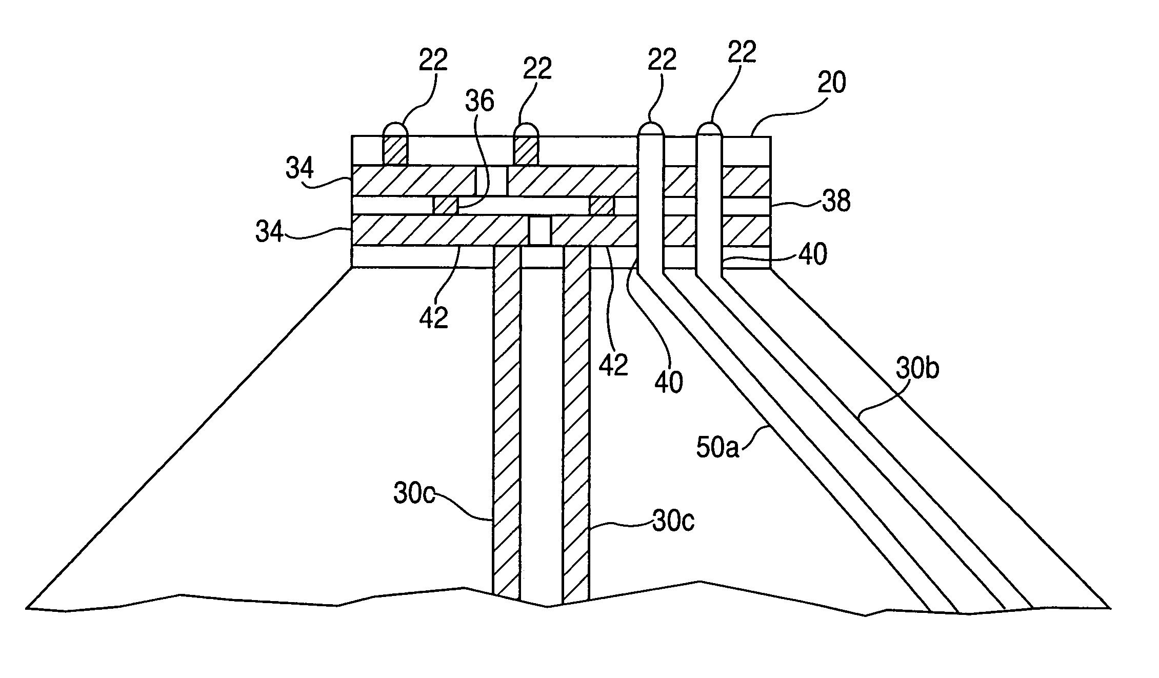
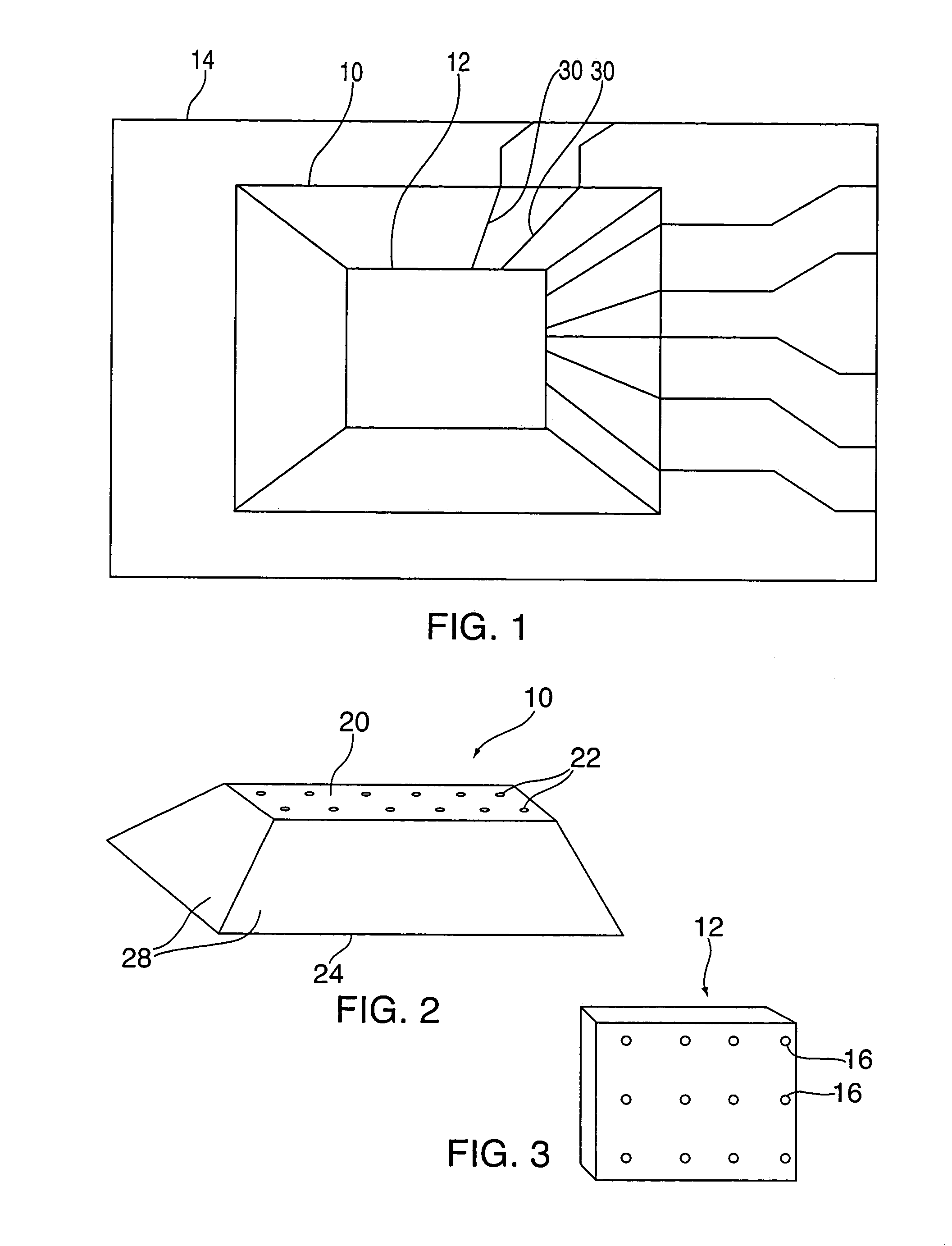
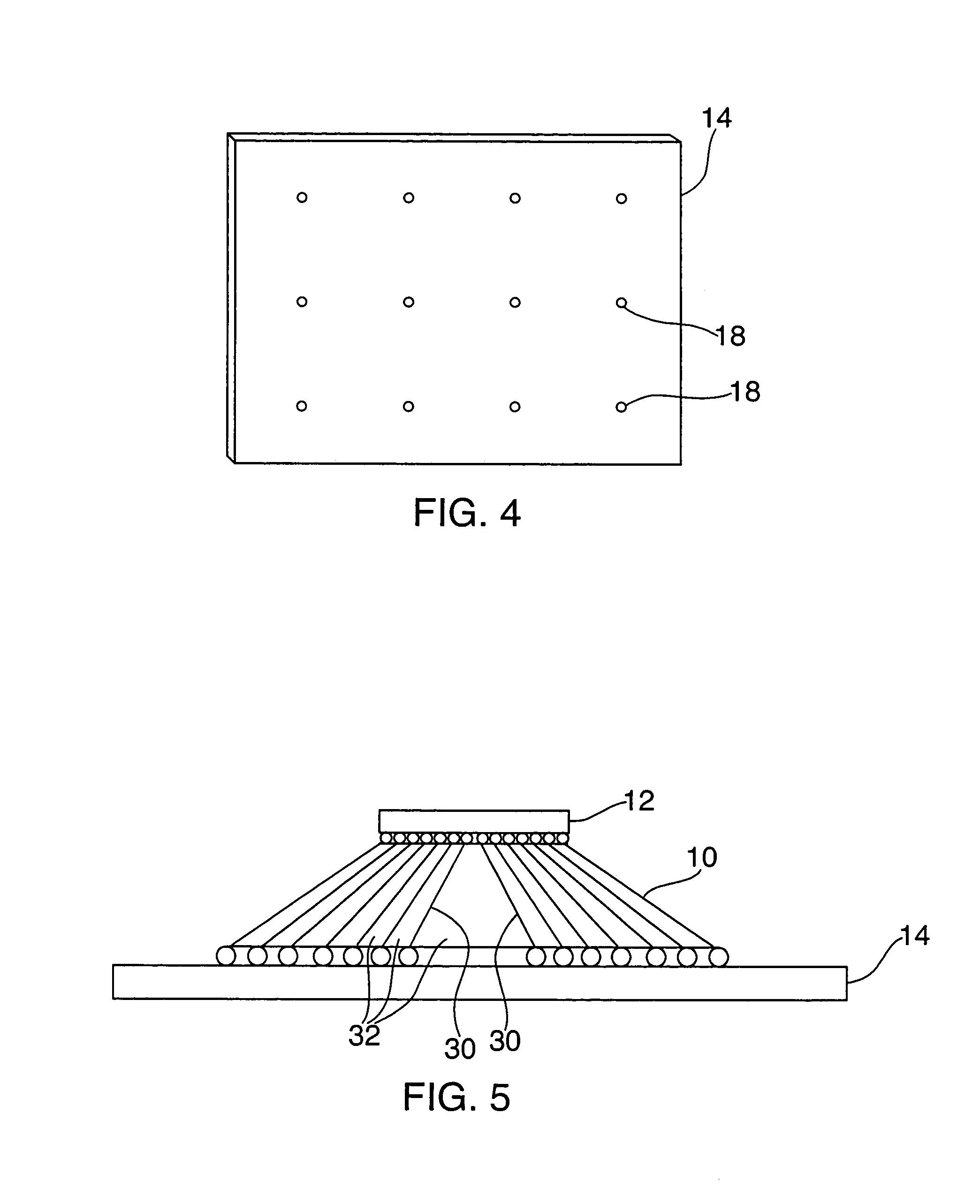
[0026]Referring now to the drawings, wherein like reference numerals refer to like parts throughout, there is seen in FIG. 1 a redistribution package, designated generally by reference numeral 10, for electrically interconnecting an integrated circuit chip 12 to an integrated circuit board 14. Chip 12 is any type of chip that is generally used in the electronics industry and includes a plurality of electrical contacts 16 (see FIG. 3) disposed on its bottom surface, such as for example, C4 connections. Board 14 is a typical integrated circuit board and is provided with a plurality of electrical contacts 18 (see FIG. 4) in a predetermined format, such as in a ball grid array (BGA). As is typical, contacts 16 are arranged in a much finer pitch pattern than are contacts 18. For example, contacts 16 may be spaced apart by about 100 μm–200 μm, while contacts 18 may be spaced no less than approximately 1 mm apart. Redistribution package 10 provides effective electrical interconnection betw...


PUM


Abstract

The present invention provides a redistribution package having an upper surface that includes contacts with reduced pitch that correspond, for example, to that of a Controlled Collapse Chip Connection (“C4”) structure formed on a chip, and a lower surface having contacts with increased pitch that correspond, for example, to a printed circuit board employing ball grid array (“BGA”) pads. A series of power, signal and ground conductors extend through the body of the redistribution package and interconnect the circuit board contacts to the chip contacts.

Description

BACKGROUND OF THE INVENTION[0001]1. Field of the Invention[0002]This invention relates to the field of integrated circuit chip packaging, and more specifically to devices for connecting an integrated circuit chip to a printed circuit board.[0003]2. Description of Prior Art[0004]Integrated circuit chips have a large number of pins that must be connected to a circuit board. The circuit board sends and receives signals from the integrated circuit chip and also provides power and ground for the chip. Integrated circuit chips are small in comparison to circuit boards and typically have pins that are separated by 100 μm to 200 μm. The circuit boards to which integrated circuit chips are connected have connector pads that typically are separated by no less than approximately 1 mm.[0005]It is necessary to provide means for connecting the closely-spaced contacts of integrated circuit chips to the more widely-spaced contacts of a circuit board. The connections between the chip and the printed...

Claims


Application Information

Patent Timeline
Patent Type & Authority Patents(United States)
IPC IPC(8): H01R12/00H01L23/498H01L23/50
CPCH01L23/49822H01L23/49827H01L23/49838H01L23/50H01L2224/16H01L2924/15159H01L2924/15174H01L2924/15311H01L2924/3011
Inventor BUDELL, TIMOTHY W.TREMBLE, ERIC W.WELCH, BRIAN P.
Owner GLOBALFOUNDRIES INC
Why Eureka
Try Eureka