Method of manufacturing III-V group compound semiconductor
a technology of compound semiconductors and nitride, which is applied in the direction of crystal growth process, polycrystalline material growth, chemically reactive gases, etc., can solve the problems of difficult to obtain high-quality crystal over a wide area, difficult to grow a large crystal, and inability to obtain crystals of a size practical for fabricating semiconductor chips. achieve the effect of improving crystallinity
- Summary
- Abstract
- Description
- Claims
- Application Information
AI Technical Summary
Benefits of technology
Problems solved by technology
Method used
Image

Examples
working examples
EXAMPLE 1
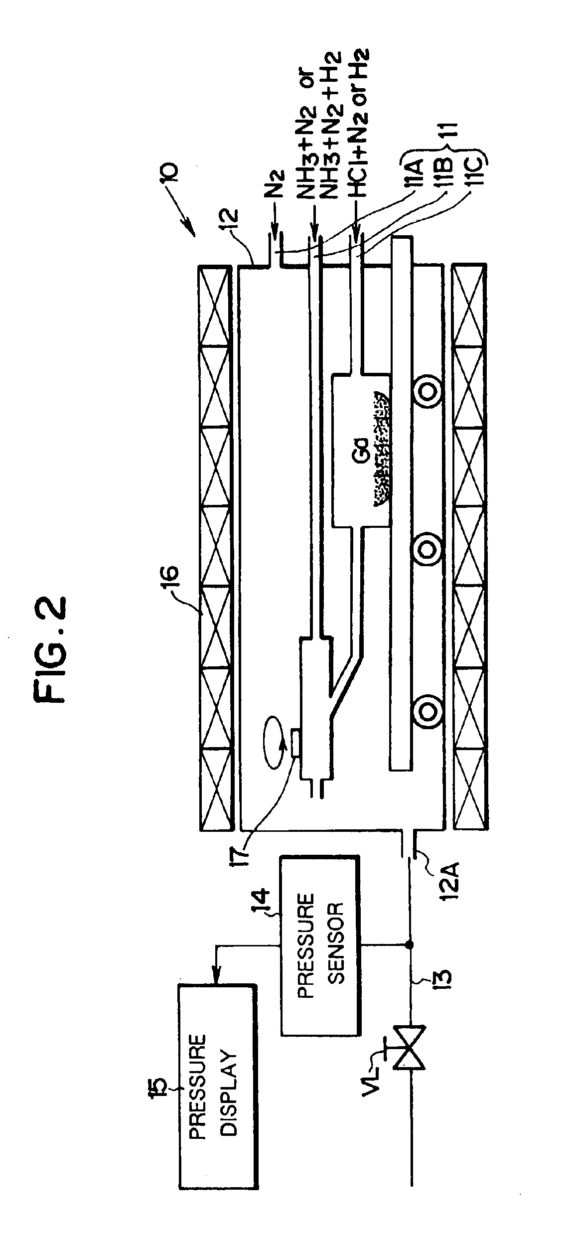
[0033]The vapor deposition semiconductor manufacturing system 10 shown in FIG. 2 was used as set out below to epitaxially grow a GaN thin film on a base layer of GaN formed on a sapphire substrate by MOVPE.
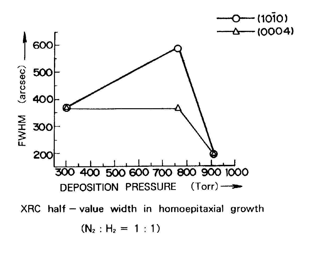
[0034]The temperature in the reactor 12 was controlled by regulating the flow rate control valve VL concomitantly with temperature increase, and the temperature profile in the reactor 12 was established as shown in FIG. 3. The starting materials were supplied at a constant V / III ratio of 25 (NH3 partial pressure: 0.2 atm, GaCl partial pressure: 8×10⁻³ atm) and growth was conducted with the internal pressure of the reactor 12 controlled to 910 Torr. As the flow rate was constant, the carrier gas flow rate was varied with pressure. The experiment was conducted using a mixed carrier gas composed of equal amounts of N2 and H2 (N2:H2=1:1). Specimens for comparison were produced at pressures of 300 Torr and 760 Torr.
[0035]The invention specimen produced at a deposition pressure...
example 2
[0037]A specimen was manufactured by growing a GaN thin film on a base layer of GaN formed on a sapphire substrate by MOVPE. The same method as in Example 1 was used expect for changing the deposition pressure to 836 Torr. The surface morphology of the specimen was observed with an optical microscope. The surface was found to be free of cracks and of excellent quality like that of Example 1. The half-value width of the (0004) and (10—10) diffractions were measured and found to be 175 seconds and 220 seconds, indicating good crystallinity on a par with that in Example 1.
[0038]As explained in the foregoing, the present invention enables manufacture of a III-V Group nitride compound semiconductor exhibiting excellent crystallinity simply by setting the deposition pressure slightly higher than atmospheric pressure when epitaxially growing a III-V Group nitride compound semiconductor by HVPE. The present invention thus offers a method of outstanding industrial value for its ability to ma...
PUM
| Property | Measurement | Unit |
|---|---|---|
| pressure | aaaaa | aaaaa |
| pressure | aaaaa | aaaaa |
| thickness | aaaaa | aaaaa |
Abstract
Description
Claims
Application Information
 - R&D Engineer
- R&D Manager
- IP Professional
- Industry Leading Data Capabilities
- Powerful AI technology
- Patent DNA Extraction
Browse by: Latest US Patents, China's latest patents, Technical Efficacy Thesaurus, Application Domain, Technology Topic.
© 2024 PatSnap. All rights reserved.Legal|Privacy policy|Modern Slavery Act Transparency Statement|Sitemap