

Film forming apparatus and film forming method
a film forming apparatus and film technology, applied in the field of film forming apparatus and film forming method, can solve the problems of insufficient life of elements, degradation of organic compound layer, mixing of impurities in organic compound, etc., and achieve the effect of high purity and reduced purity of purified organic compound
- Summary
- Abstract
- Description
- Claims
- Application Information
AI Technical Summary
Benefits of technology
Problems solved by technology
Method used
Image

Examples
embodiment mode 1
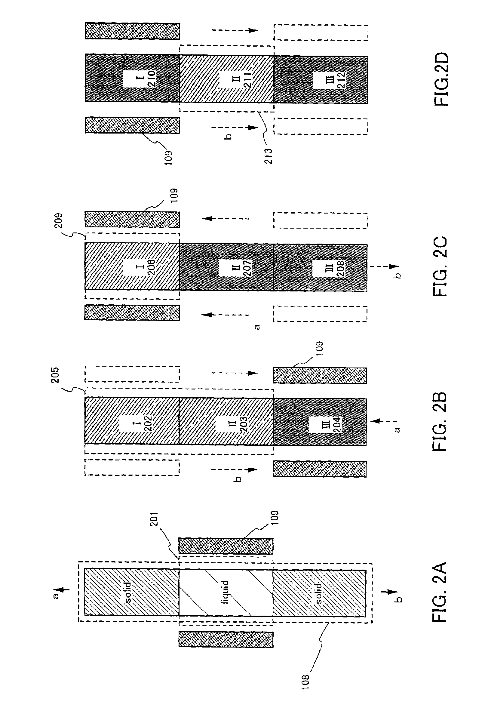
[0043]In Embodiment Mode 1 of the present invention, the structures of a film forming chamber and a purifying chamber of a film forming apparatus will be described with reference to FIG. 1.
[0044]A film forming chamber 101 and a purifying chamber 102 are connected to each other via a gate 103. The purifying chamber 102 is disposed under the film forming chamber 101. The film forming chamber 101 is kept in a reduced-pressure state or a vacuum state by an exhaust system 106. In contrast, the purifying chamber 102 is generally kept in an atmospheric state during purification. Furthermore, a substrate 105 is disposed in the film forming chamber 101 by a substrate holder 104. The substrate 105 includes the state where a thin film is formed on the surface thereof.
[0045]A crucible 108 and a heater 109 are provided in the purifying chamber 102. The crucible 108 is provided with a solid organic compound serving as a material for forming an organic compound layer. Although not shown here, it m...
embodiment mode 2
[0060]FIG. 3 shows structures of a film forming chamber and a purifying chamber of a film forming apparatus in Embodiment Mode 2 of the present invention.
[0061]A film forming chamber 301 and a purifying chamber 302 are connected to each other via a gate 303. The film forming chamber 301 is kept in a reduced-pressure state or a vacuum state by an exhaust system 310. In contrast, the purifying chamber 302 is generally kept in an atmospheric state during purification. Furthermore, a substrate 305 is disposed in the film forming chamber 301 by a substrate holder 304. The substrate 305 includes the state where a thin film is formed on the surface thereof.
[0062]In the film forming chamber 301, a vaporization source 306 including an organic compound is disposed, and the organic compound vaporized by heating in a vaporization source 306 is evaporated onto the substrate 305 by opening a shutter 307. For heating of the organic compound in the vaporization source 306, resistance heating is use...
embodiments
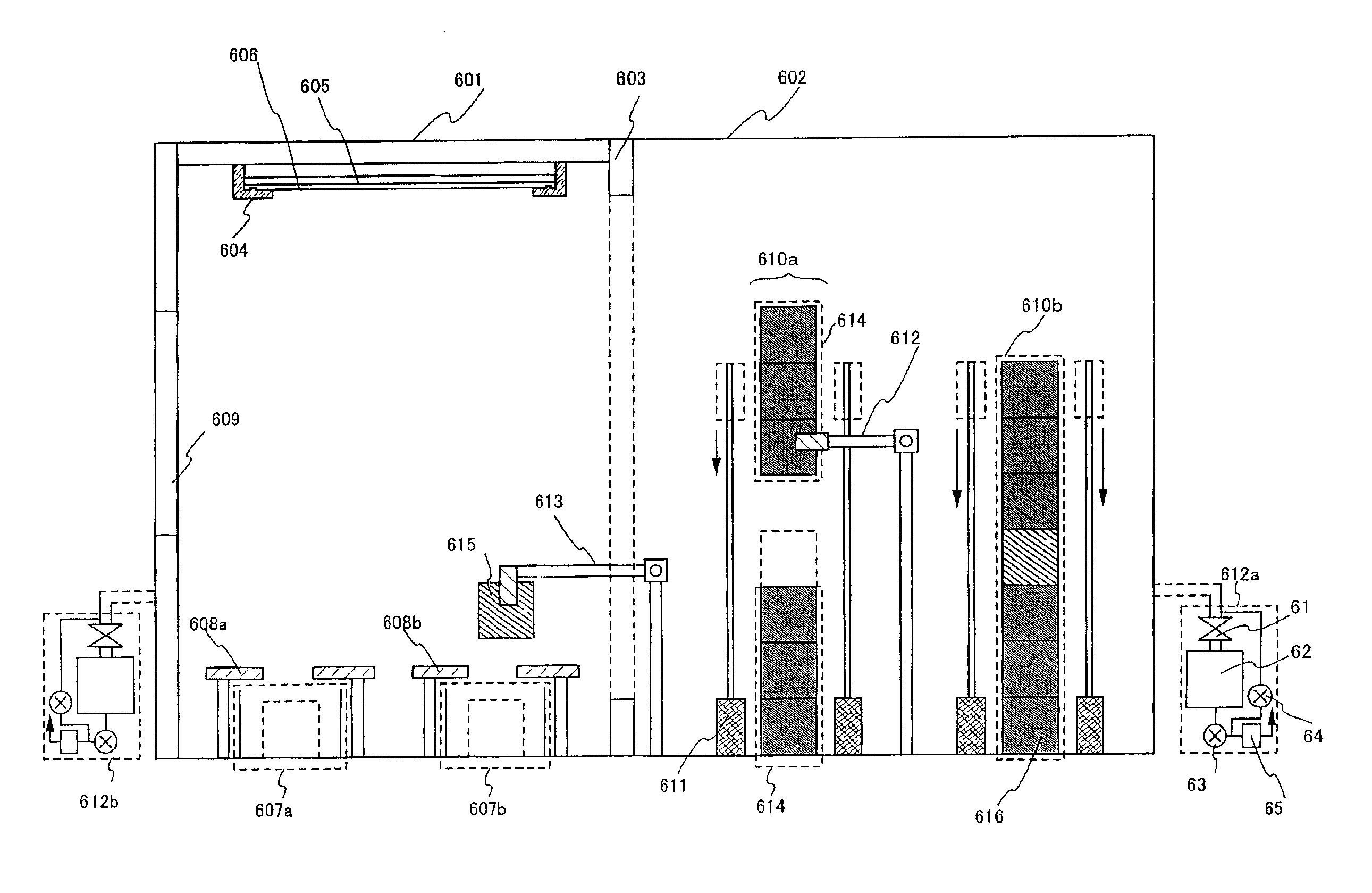
Embodiment 1
[0084]In the present embodiment, a method will be described in which vapor deposition is conducted onto a substrate provided in a film forming chamber, using a vaporization source obtained by heating an organic compound for forming a high-purity region by a heater among an organic compound provided in a crucible in a purifying chamber, as described in Embodiment Mode 1.
[0085]FIG. 5 shows cross-sectional structures of a film forming chamber and a purifying chamber in a film forming apparatus of the present embodiment. In FIG. 5, a film forming chamber 501 and a purifying chamber 502 are connected to each other via a gate 503. The purifying chamber 502 is disposed under the film forming chamber 501. In the film forming chamber 501, a substrate 505 is disposed by a substrate holder 504. The substrate 505 includes the state where a thin film is formed on the surface thereof.
[0086]A metal mask 506 is provided in the vicinity of the substrate 505, and the metal mask 506 is sup...
PUM
| Property | Measurement | Unit |
|---|---|---|
| speed | aaaaa | aaaaa |
| temperature | aaaaa | aaaaa |
| surface roughness | aaaaa | aaaaa |
Abstract
Description
Claims
Application Information