Method for providing nano-structures of uniform length

a nano-structure, uniform technology, applied in the field of nanotechnology, can solve the problems of insufficient length, insufficient length, and insufficient efficiency of electron transport between nano-devices, and achieve the effect of more precise cutting

Inactive Publication Date: 2005-09-20
EI DU PONT DE NEMOURS & CO
View PDF4 Cites 189 Cited by
  • Summary
  • Abstract
  • Description
  • Claims
  • Application Information

AI Technical Summary

Problems solved by technology

The increasing complexity of electronic devices, and integrated circuits, coupled with the decreasing size of individual circuit elements, place ever more stringent demands on fabrication processes, particularly with respect to resolution and accuracy of the fabrication patterns.
Such a variation in electrical properties may adversely affect the efficiency of electron transport between nano-devices interconnected by the carbon nanotube.
However, existing technology does not provide a means for producing nanotubes of either uniform length, or a well-defined range of length distributions, nor does it provide a means for the rapid and controlled cutting of nanotubes to specific dimensions.
The method is effective for the cutting of a single CNT however suffers from some significant deficiencies such as an empirical ion selection process and an inability to control the size and length of the newly generated CNT's.
The method is labor intensive requiring intensive ultrasonic-homogenization in the presence of a polymer solution, filtration, and purification steps and is limited to only single-wall carbon nanotubes.
The methods described above may be applied to cut CNT's and other nanostructures on a small scale however are not easily adapted for industrial scale CNT modification.
Additionally these methods suffer from the limitation of being unable to reproduciblye generate populations of nanostructures having uniform physical parameters of length, width, diameter and area.

Method used


Image

  • Method for providing nano-structures of uniform length
  • Method for providing nano-structures of uniform length
  • Method for providing nano-structures of uniform length

Examples


example 1

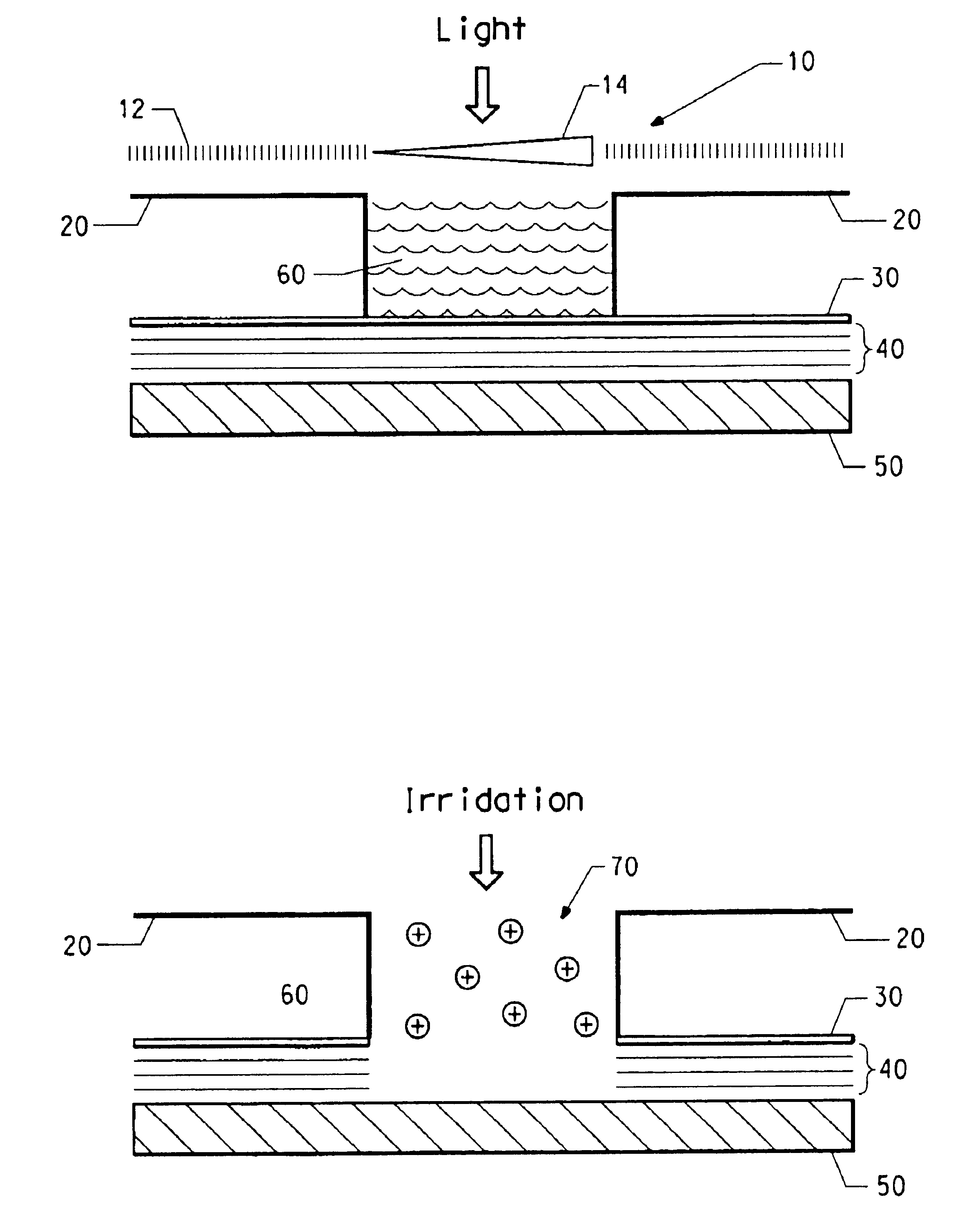
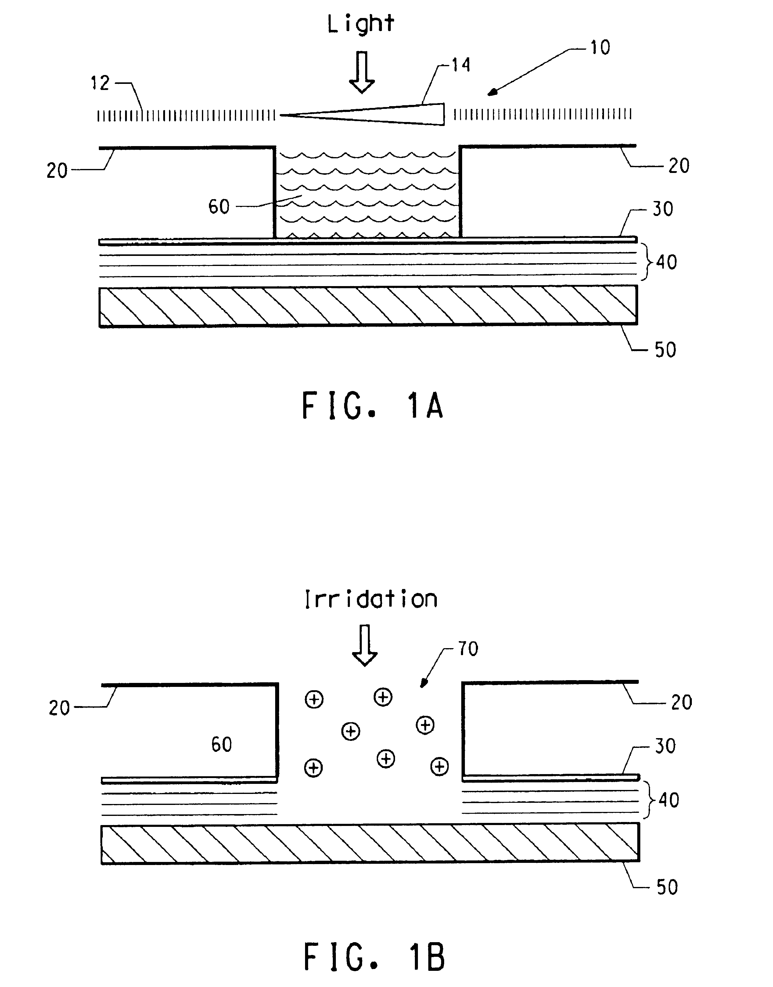
Application of a Positive Resist to Nanotube Cutting Using a Polymeric Matrix as the Dispersant Layer

[0186]A dispersion of 0.1% (w / w) carbon nanotubes in Shipley (Marlborough, Mass.) AR2 antireflective coating (ARC), was prepared by sonication in a water bath for 8 hours. This dispersion was spun onto a 4 inch silicon wafer at a speed of 2600 RPM for 30 seconds, then the wafer was baked at 205° C. for 1 minute. Shipley positive photoresist UV 113.4 was spun onto the wafer at a speed of 2800 RPM for 30 s. The wafer was then baked at 135° C. for 1 minute. The coated wafer was exposed through a standard resolution pattern photomask with 248 nm light at an intensity of 55 mJ / cm2 (using a Nikon NSR 1505 EX-1 stepper Tokyo, Japan). The exposed wafer was baked at 130° C. for 90 seconds, then developed for 45 s in AZ 300 MIF an aqueous base developer (Clariant Corp., Somerville, N.J.), rinsed with deionized water, and dried with filtered nitrogen. This left the dispersant layer revealed in ...

example 2

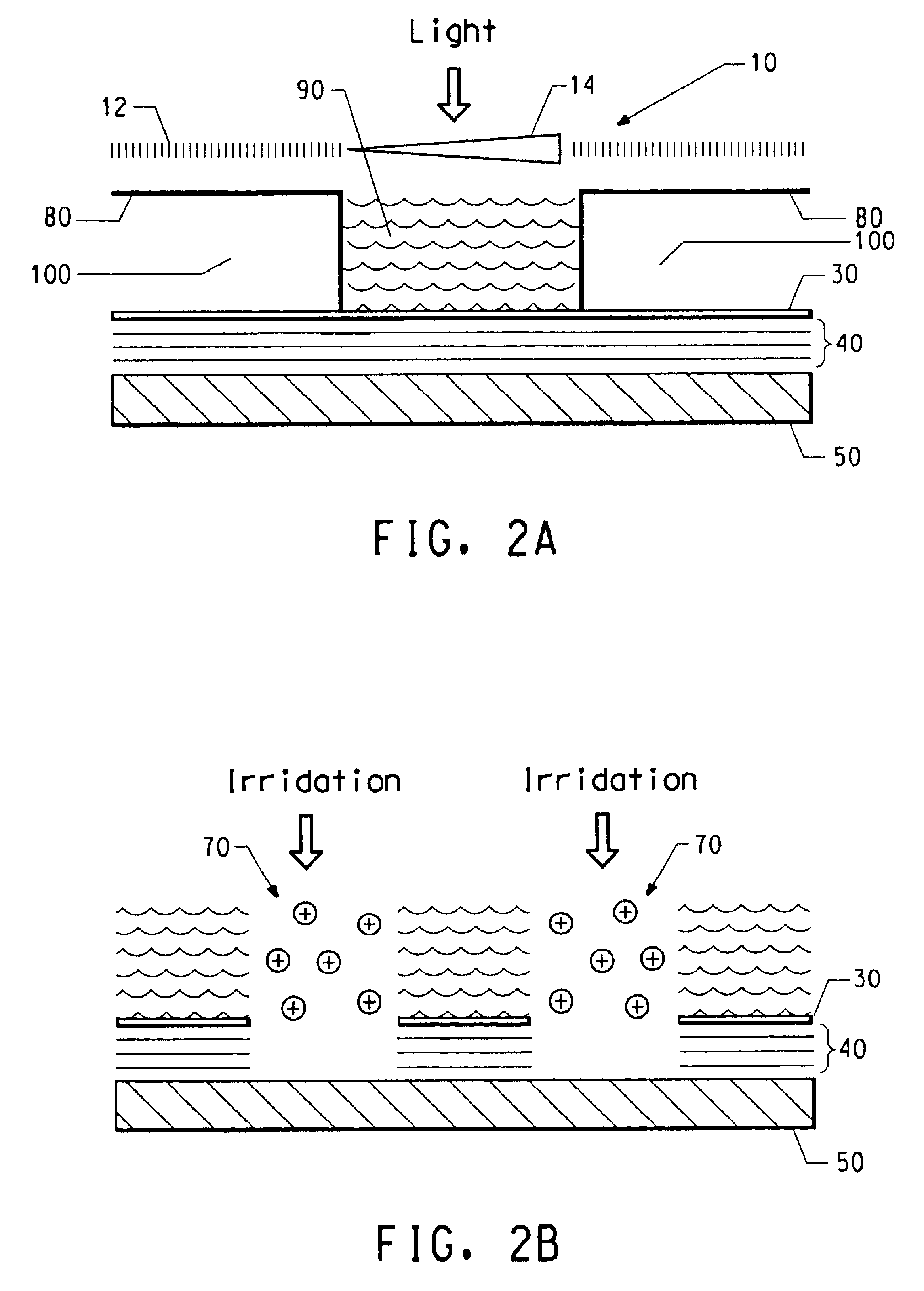
Application of a Positive Resist to Nanotube Cutting Using a Different Polymeric Matrix as the Dispersant Layer

[0189]A dispersion of 0.01% (w / w) carbon nanotubes in Brewer DUV 52 antireflective coating (ARC) (Brewer Science, Inc., Rolla, Mo.), was prepared by sonication. This dispersion was spun onto a 4 inch silicon wafer at a speed of 6000-6200 RPM for 30 seconds, then the wafer was baked at 205° C. for 1 minute. Shipley positive photoresist UV 113.4 was spun onto the wafer at a speed of 2800 RPM for 30 s. The wafer was then baked at 135° C. for 1 minute. The coated wafer was exposed through a patterned photomask with 248 nm light at an intensity of 25 mJ / cm2 (using a Nikon NSR 1505 EX-1 stepper Tokyo, Japan). The exposed wafer was baked at 130° C. for 60-90 seconds, then developed for 45 s in AZ 300 MIF an aqueous base developer (Clariant Corp., Somerville, N.J.), rinsed with deionized water, and dried with filtered nitrogen. This left the dispersant layer revealed in the uv-expo...

example 3

Application of a Negative Resist to Nanotube Cutting Using a Polymeric Matrix as the Dispersant Layer

[0192]Carbon nanotubes were dispersed in 20 mL Shipley AR2 antireflective coating and sonicated in a water bath for 12 hours. This dispersion was spun onto a 4 inch silicon wafer at a speed of 2600 RPM for 30 seconds, then the wafer was baked at 205° C. for 1 minute. Shipley negative photoresist UVN30 was spun onto the dispersant layer of the wafer at a speed of 3000 RPM for 30 s. The wafer was then baked at 110° C. for 1 minute. The coated wafer was exposed through a standard resolution pattern photomask with 248 nm light at an intensity of 28.5 mJ / cm2 (using a Nikon NSR 1505 EX-1 stepper). The exposed wafer was baked at 105° C. for 60 seconds, then developed for 30 seconds in AZ 300 MIF developer, rinsed with DI water, and dried with filtered nitrogen. This left the dispersant layer revealed in the UV-unexposed regions. Wafer 154 was etched in a 90 W oxygen plasma for 30 seconds us...


PUM

PropertyMeasurementUnit
lengthaaaaaaaaaa
lengthaaaaaaaaaa
lengthaaaaaaaaaa

Abstract

This invention relates to the field of nanotechnology. Specifically the invention describes a method for cutting a multiplicity of nano-structures to uniform dimensions of length, length and width, or area, or to a specific distribution of lengths or area using various cutting techniques.

Description

[0001]This application claims the benefit of U.S. Provisional Application 60 / 370576, filed Apr. 5, 2002.FIELD OF INVENTION[0002]This invention relates to the field of nanotechnology. Specifically the invention describes a method for cutting a multiplicity of nano-structures, and particularly nanotubes to uniform dimensions of length, width, diameter or area.BACKGROUND OF THE INVENTION[0003]The increasing complexity of electronic devices, and integrated circuits, coupled with the decreasing size of individual circuit elements, place ever more stringent demands on fabrication processes, particularly with respect to resolution and accuracy of the fabrication patterns. The ability to fabricate on a nanometer scale guarantees a continuation in miniaturization of functional devices, in for example, in microelectronic circuitry as well as other applications.[0004]One class of nano-structures are carbon nanotubes (CNT's) which have attracted much attention because of their dimensions and pr...

Claims


Application Information

Patent Timeline
Patent Type & Authority Patents(United States)
IPC IPC(8): C01B31/00C01B31/02B82B3/00B82B1/00
CPCB82Y30/00B82Y40/00C01B31/0273C01B31/028C01B2202/34Y10S977/84Y10S977/856Y10S977/889C01B32/174C01B32/176
Inventor FRENCH, ROGER HARQUAILGIERKE, TIMOTHYHARMER, MARK ANDREWJAGOTA, ANANDLUSTIG, STEVEN RAYMONDMEHTA, RAKESH H.HIETPAS, PAULA BEYERONOA, BIBIANA
Owner EI DU PONT DE NEMOURS & CO
Why Eureka
Try Eureka