
Pre-patterned substrate for organic thin film transistor structures and circuits and related method for making same

Inactive Publication Date: 2005-09-20
RPX CORP
View PDF5 Cites 39 Cited by
  • Summary
  • Abstract
  • Description
  • Claims
  • Application Information

AI Technical Summary

Benefits of technology

[0010]The use of organic thin film transistors (OTFTs) in electronic devices lends itself to the mass manufacturing of the devices at a lower cost and in a shorter time frame for many applications. The use of OTFTs in mobile telephones for example, provide new “design” or feature opportunities and a solution for a higher degree of integration and added functionality into the electronic device covers which can be changed from device to device (inter-exchangeable covers), as well as a simplified I / O interface between the cover and the device. Furthermore, the use of organic transistors would facilitate the manufacture and use of thin flexible circuits.
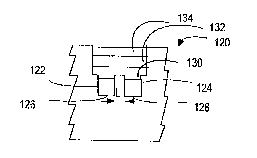
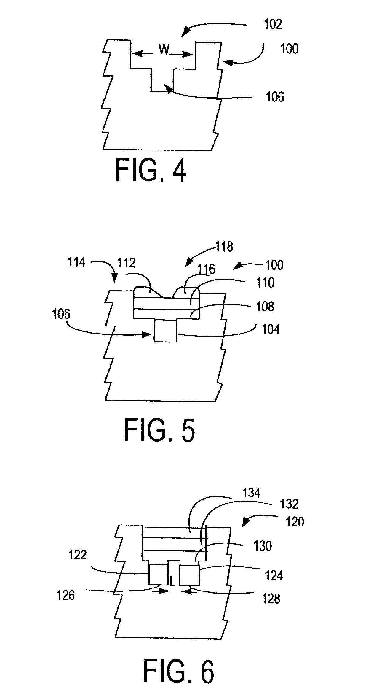
[0011]Using substrates with pre-defined grooves or patterns in the substrate surface for receiving organic semiconducting material and organic conductive circuits on the substrate is less complex than currently known methods that use chemical barriers or surface treatment to define the organic material receiving area. Furthermore, because the organic circuit material deposited in the grooves or patterns would not extend or protrude beyond the surface of the substrate, but rather be inserted into the substrate, the risk of damaging the organic circuit by mechanical rubbing, etc, is minimized if not substantially eliminated.

Problems solved by technology

Possible sources for size and cost reduction are the traditional electronic circuits / chips that are used and which can be unproportionally expensive in low cost applications.
The performance of a printed OTFT is usually not as good as the performance of a vacuum deposited OTFT.
Nonetheless, the performance of a printed OTFT structure is more than adequate for low frequency applications.
However, there is one drawback with the ink-jet printing of OTFT structures and circuits that is a result of the spreading of the ink-jet droplet when it hits the surface.
The pre-patterning of a substrate using chemical barriers and the like as known to those skilled in the art for the depositing of organic materials on a substrate is an additional process that increases the cost of the technology used to apply the organic and inorganic material to the substrate surface.

Method used


Image

  • Pre-patterned substrate for organic thin film transistor structures and circuits and related method for making same
  • Pre-patterned substrate for organic thin film transistor structures and circuits and related method for making same
  • Pre-patterned substrate for organic thin film transistor structures and circuits and related method for making same

Examples


Embodiment Construction

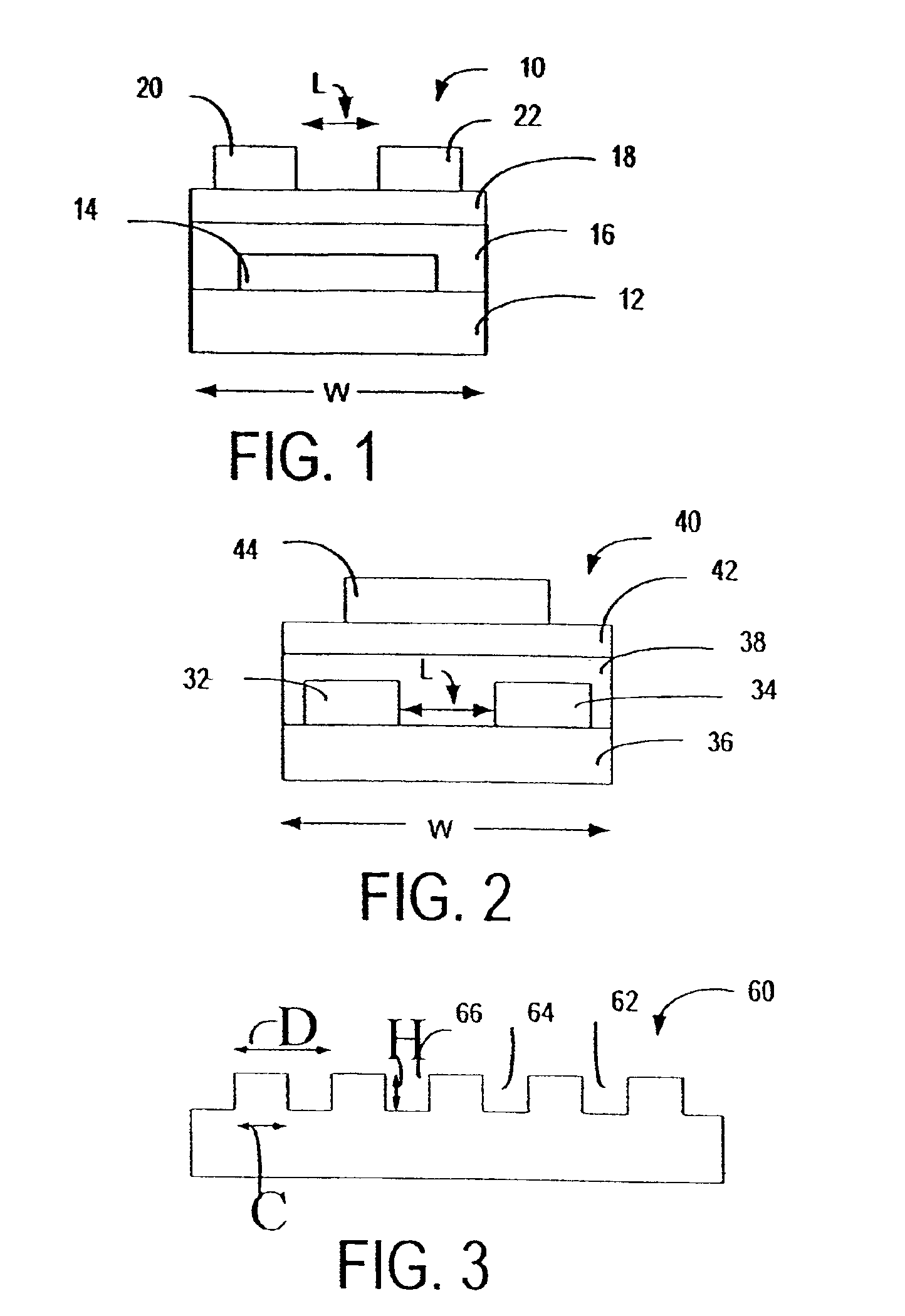
[0038]Turning now to the drawings and considering the invention in further detail, an organic thin film transistor (OTFT) structure having a bottom gate configuration is illustrated in FIG. 1 and is generally designated 10. An organic thin film transistor (OTFT) structure having a top gate configuration is illustrated in FIG. 2 and is generally designated 40. As described above, the OTFT structure is deposited on a substrate 12 and in the case of the bottom gate configuration shown in FIG. 1, the gate 14 is deposited on the substrate 12 and is surrounded by an insulating layer 16. An organic semiconductor layer 18 is deposited on the insulating layer 16. The source 20 and the drain 22 are deposited on the organic semiconductor layer 18 and are spaced from one another a distance L.

[0039]In the case of a top gate OTFT structure configuration, as illustrated in FIG. 2, the source 32 and the drain 34 electrodes are deposited on the substrate 36 and are spaced a distance L from one anoth...


PUM


Abstract

Grooves in a desired circuit configuration are formed in the surface of a substrate to pre-pattern the area to receive material forming an organic thin film transistor (OTFT) structure and interconnecting conductive paths. The OTFT material is deposited in the pre-patterned area using printing techniques such as ink jet printing. In one embodiment, the grooves are formed in the surface substrate during the injection molding process of the substrate. Inter-exchangeable device covers carry different substrates to provide different functionalities of an electronic device with which the covers are used.

Description

TECHNICAL FIELD[0001]The present invention relates generally to organic thin film transistor (OTFT) structures and organic circuits employed in user interfaces and input / output arrangements and deals more particularly with a pre-patterned substrate for receiving the OTFT structures and organic circuits. The invention further relates to a method for applying the organic semiconductor material and conductive material on the substrate using reel-to-reel manufacturing processes to produce the OTFT structure and organic circuit. The invention also deals with a method for defining and producing the pre-patterned areas for receiving the material forming the OTFT structure and organic circuit during the injection molding process of a substrate. The invention also deals with the inter-exchangeability of component structural elements carrying different substrates to provide different functionalities of a device with which the component structural elements are used.BACKGROUND OF THE INVENTION[...

Claims


Application Information

Patent Timeline
IPC IPC(8): H01L51/40H01L51/00H01L51/05
CPCH01L51/00H01L51/0005H01L51/0512H01L51/0545H10K99/00H10K71/135H10K10/462H10K10/466
Inventor OSTERGARD, TONI
Owner RPX CORP
Learn More