
Lateral short-channel DMOS, method of manufacturing the same, and semiconductor device
a technology of short-channel dmos and manufacturing methods, applied in the direction of semiconductor devices, electrical equipment, basic electric elements, etc., can solve the problems of high resistance, achieve low resistance, reduce resistance, and stabilize breakdown characteristics
- Summary
- Abstract
- Description
- Claims
- Application Information
AI Technical Summary
Benefits of technology
Problems solved by technology
Method used
Image

Examples
embodiment 1
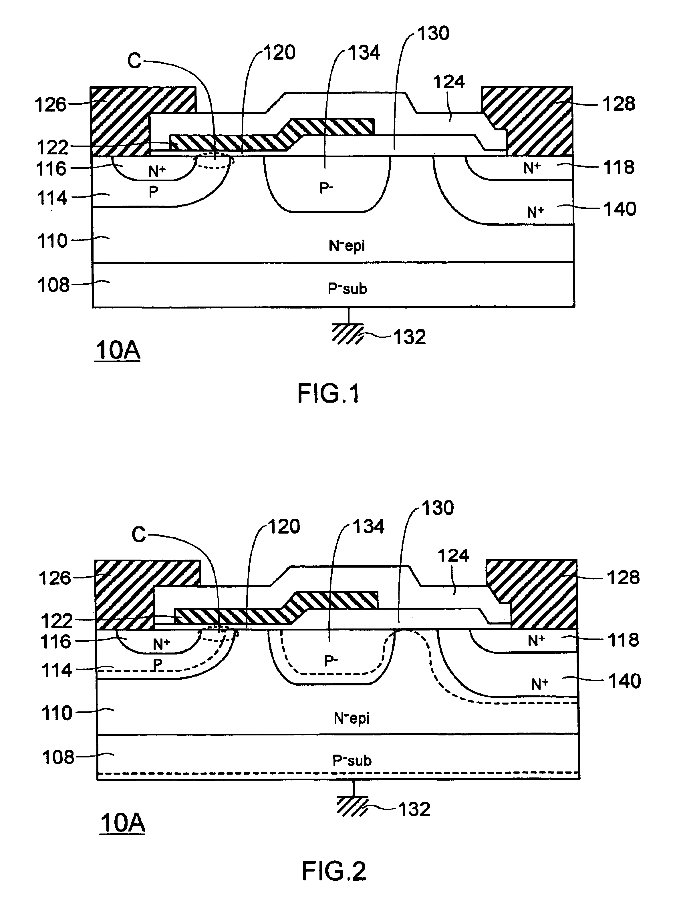
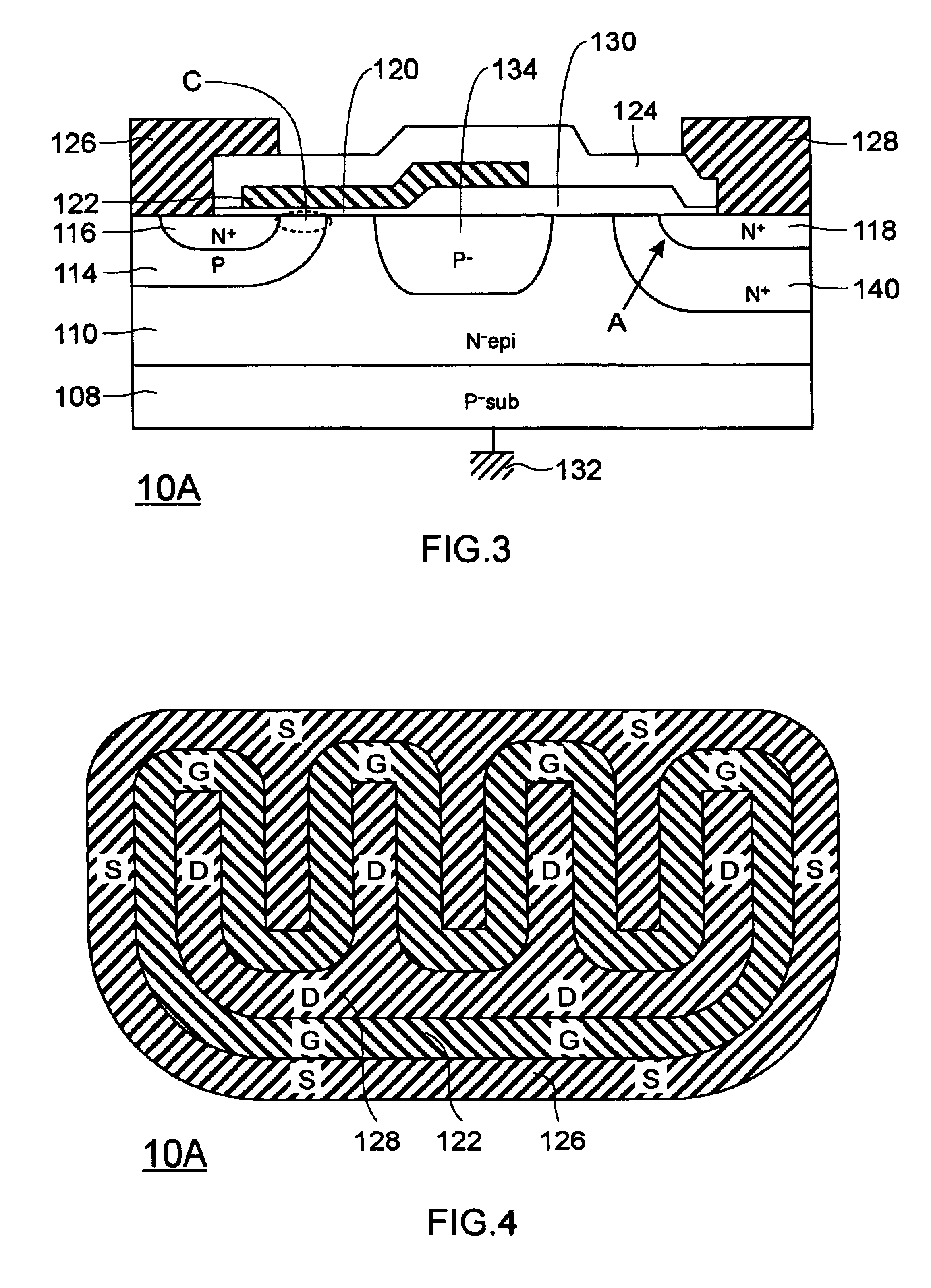
[0081]FIG. 1 is a cross-sectional view of a lateral short-channel DMOS according to Embodiment 1. FIGS. 2 and 3 are diagrams useful in explaining operational effects of the lateral short-channel DMOS according to Embodiment 1. FIG. 4 is a plan view of the lateral short-channel DMOS according to Embodiment 1.
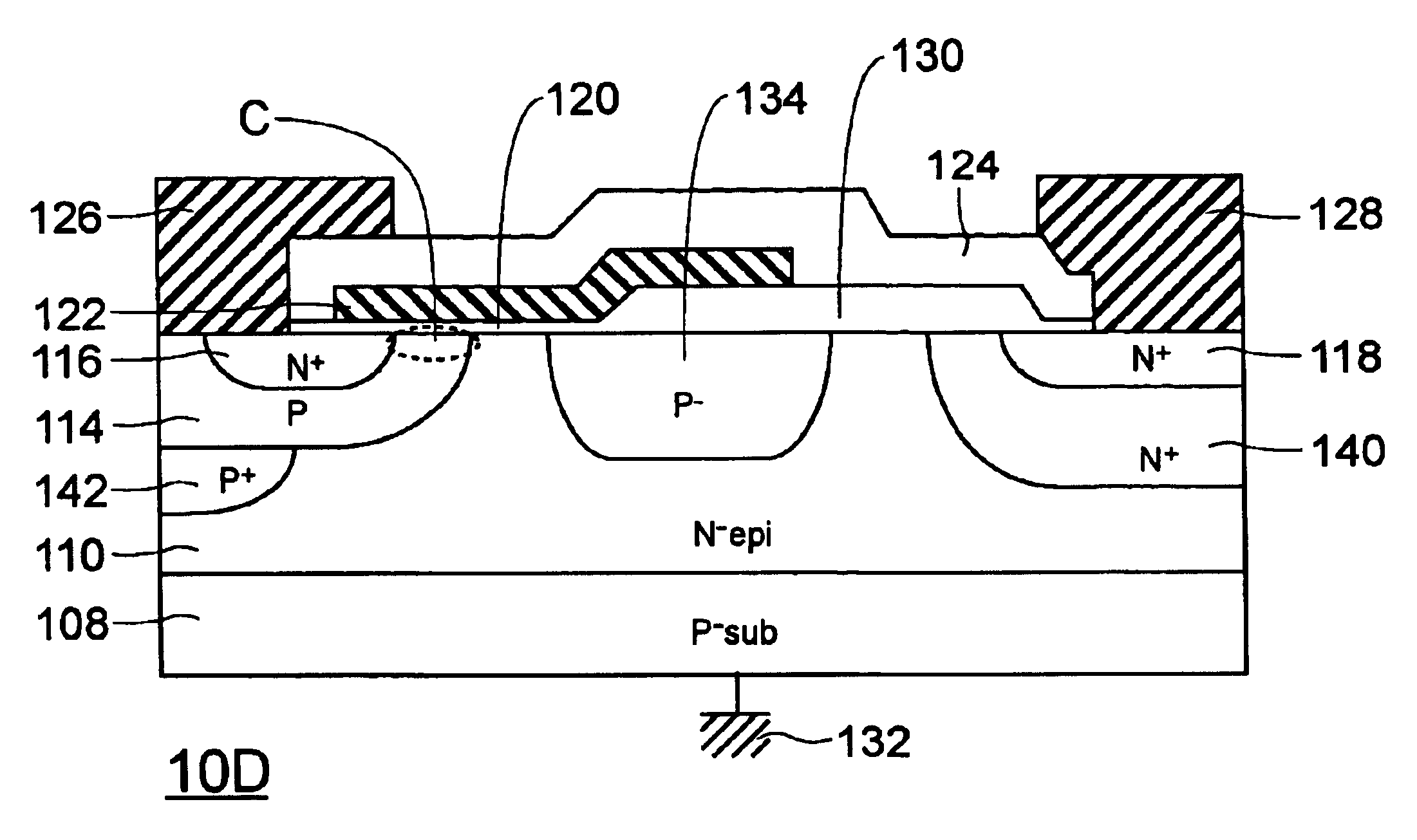
[0082]As shown in FIG. 1, a lateral short-channel DMOS 10A according to Embodiment 1 has an N−-type epitaxial layer (first conductivity-type semiconductor region) 110 formed on one surface of a P−-type semiconductor substrate (semiconductor substrate) 108, and as shown in FIG. 2 is a so-called RESURF-type lateral short-channel DMOS in which the surface of the N−-type epitaxial layer 110 is almost completely depleted during reverse bias.
[0083]In this lateral short-channel DMOS 10A, a P-type well (second conductivity-type well) 114 including a channel forming region C is formed in the surface of the N−-type epitaxial layer 110, and an N+-source region (first conductivity-type sourc...
embodiment 2
[0097]FIG. 5 is a cross-sectional view of a lateral short-channel DMOS according to Embodiment 2. A lateral short-channel DMOS 10B according to Embodiment 2 has a similar structure to the lateral short-channel DMOS 10A according to Embodiment 1, but differs as shown in FIG. 5 in that an N−-type diffused region 136 including a higher concentration of N-type dopant than the N−-type epitaxial layer 110 is also formed in an N−-type epitaxial layer 110 surface side of the P−-type diffused region 134.
[0098]This means that according to the lateral short-channel DMOS 10B according to Embodiment 2, in addition to the effects of the lateral short-channel DMOS 10A according to Embodiment 1, the following effect is obtained. That is, the current from the N+-type drain region 118 to the N+-type source region 116 when the DMOS 10B is ON flows in a deeper part (the N−-type epitaxial layer 110) than the P−-type diffused region 134 and also flows in part of the N−-type diffused region 136 that has r...
embodiment 3
[0100]FIG. 6 is a cross-sectional view of a lateral short-channel DMOS according to Embodiment 3. A lateral short-channel DMOS 10C according to Embodiment 3 has a similar structure to the lateral short-channel DMOS 10B according to Embodiment 2, but differs as shown in FIG. 6 in that the N−-type diffused region 136 contacts the N+-type well 140.
[0101]According to the lateral short-channel DMOS 10C according to Embodiment 3, in addition to the effects of the lateral short-channel DMOS 10B according to Embodiment 2, the following effect is obtained. That is, the ON resistance of a current path from the N+-type well 140 to the N−-type diffused region 136 can be reduced further.
PUM
 Abstract
Description
Claims
Application Information