Level shift circuit and semiconductor integrated circuit

Inactive Publication Date: 2005-09-20
RENESAS ELECTRONICS CORP +1
View PDF13 Cites 21 Cited by
  • Summary
  • Abstract
  • Description
  • Claims
  • Application Information

AI Technical Summary

Benefits of technology

[0035]Preferably, the first level conversion circuit may be provided on the path of transmitting usual operational signals and the second level conversion circuit, on the path of transmitting testing signals. Sinc

Problems solved by technology

As a result, on the part of a circuit to receive a signal from such a level conversion circuit, the signal should be accepted at the later signal timi

Method used


Image

  • Level shift circuit and semiconductor integrated circuit
  • Level shift circuit and semiconductor integrated circuit
  • Level shift circuit and semiconductor integrated circuit

Examples


Embodiment Construction

[0049]Preferred embodiments of the present invention will be described below with reference to the accompanying drawings.

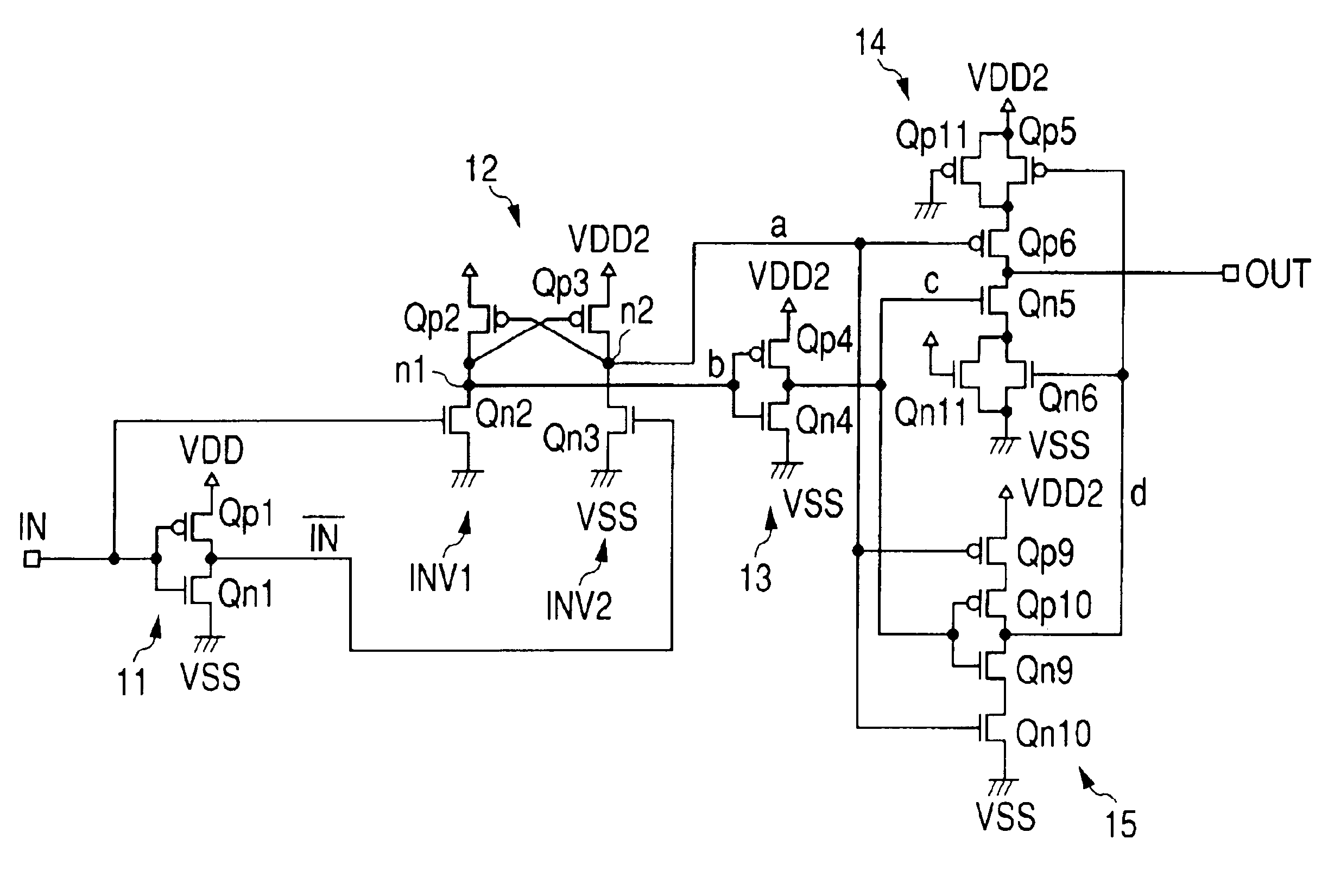
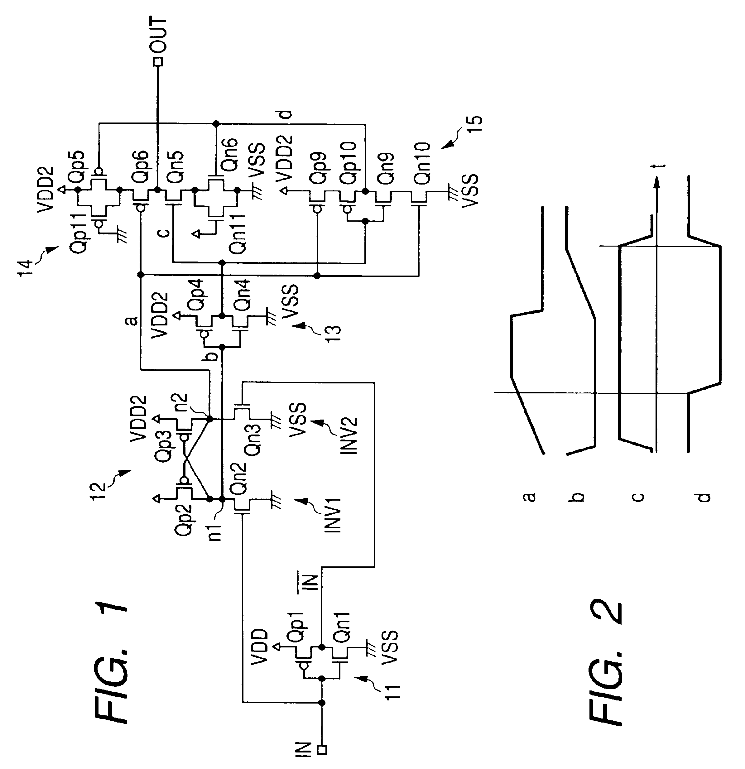
[0050]FIG. 1 is a circuit diagram of a level conversion circuit, which is a first preferred embodiment of the invention. In FIG. 1, a sign used for denoting MOSFETs denotes a p-channel MOSFET if its gate terminal position is marked with a small circle or, if not, an n-channel MOSFET.

[0051]The level conversion circuit of FIG. 1 is configured of a first stage inverter 11 for inverting an input signal IN, a latch circuit type level shift stage 12 whose inputs are a signal / IN inverted by the inverter 11 and the pre-inversion signal IN, another inverter 13 for inverting a signal on the inverted output node n1 side of the level shift stage 12, an inverter type output stage 14 whose inputs are the output signal of the inverter 13 and a signal on the non-inverted output node n2 side of the level shift stage 12, and a delay stage 15 for controlling the output stage 14 by ...


PUM


Abstract

A level conversion circuit is composed of a level shift circuit for supplying a level-converted signal in the same phase as the input signal and a signal in the reverse phase thereto and a follow-up circuit responsive to the earlier of the output signals of the level shift circuit for generating an output signal, wherein the follow-up circuit consists of an inverter circuit in which two p-channel type MOS transistors and two n-channel type MOS transistors are connected in series between a first voltage terminal and a second voltage terminal, of which one pair is used as input transistors and the remaining pair of transistors are subjected to feedback based on the output signal of the level shift circuit to be quickly responsive to the next variation.

Description

CROSS-REFERENCE TO RELATED APPLICATIONS[0001]This application is a Continuation application of U.S. application Ser. No. 09 / 976,052 filed Oct. 15, 2001, now U.S. Pat. No. 6,774,695. Priority is claimed based on U.S. application Ser. No. 09 / 976,052 filed Oct. 15, 2001, which claims priority to Japanese Patent Application No. 2000-330385 filed on Oct. 30, 2000.BACKGROUND OF THE INVENTION[0002]The present invention relates to a semiconductor integrated circuit and to a level conversion circuit, and more particularly, for instance, to a technology which can be effectively used for an interface circuit for a semiconductor integrated circuit in which the amplitude of internal signals and that of external signals differ from each other.[0003]According to the prior art, circuits for converting signals of a smaller amplitude into signals of a greater amplitude include, for instance, a level conversion circuit disclosed in Japanese Patent Laid-Open No. Hei 5(1993)-343979, the circuit illustra...

Claims


Application Information

Patent Timeline
IPC IPC(8): H03K19/003H01L21/822H01L21/8238H01L27/04H01L27/092H03K19/0175H03K19/0185
CPCH03K19/00323H03K19/0175
Inventor HAYASHI, HIROKATSUTAKAHASHI, TOSHIRO
Owner RENESAS ELECTRONICS CORP
Why Eureka
Try Eureka