Temperature-insensitive bias circuit for high-power amplifiers

a bias circuit and amplifier technology, applied in the field of semiconductor devices, can solve the problem of significantly insensitive amplifier quiescent curren

Inactive Publication Date: 2005-09-20
SKYWORKS SOLUTIONS INC
View PDF2 Cites 17 Cited by
  • Summary
  • Abstract
  • Description
  • Claims
  • Application Information

AI Technical Summary

Benefits of technology

[0008]As a result of the above arrangement, an emitter size ratio of the first bipolar transistor to the second bipolar transistor is independent of an emitter size ratio of the third bipolar transistor to the fourth bipolar transistor, thereby allowing the die area consumed by the transistors of the bias circuit to be significantly reduced.
[0010]According to another embodiment, the bias circuit further comprises a high-temperature gain compensation circuit connected in parallel with the first resistor and is configured to draw current at high temperatures. According to one particular embodiment, the high-temperature gain compensation circuit comprises a second resistor and a Schottky diode, wherein a first end of the second resistor is connected to the reference voltage, a second end of the second resistor is connected to an anode of the Schottky diode, and a cathode of the Schottky diode is connected to the first node. As discussed below, this particular arrangement provides compensation for amplifier gain drop during high temperatures.

Problems solved by technology

As discussed below, this particular arrangement results in an amplifier quiescent current which is significantly insensitive to temperature variations.

Method used


Image

  • Temperature-insensitive bias circuit for high-power amplifiers
  • Temperature-insensitive bias circuit for high-power amplifiers
  • Temperature-insensitive bias circuit for high-power amplifiers

Examples


Embodiment Construction

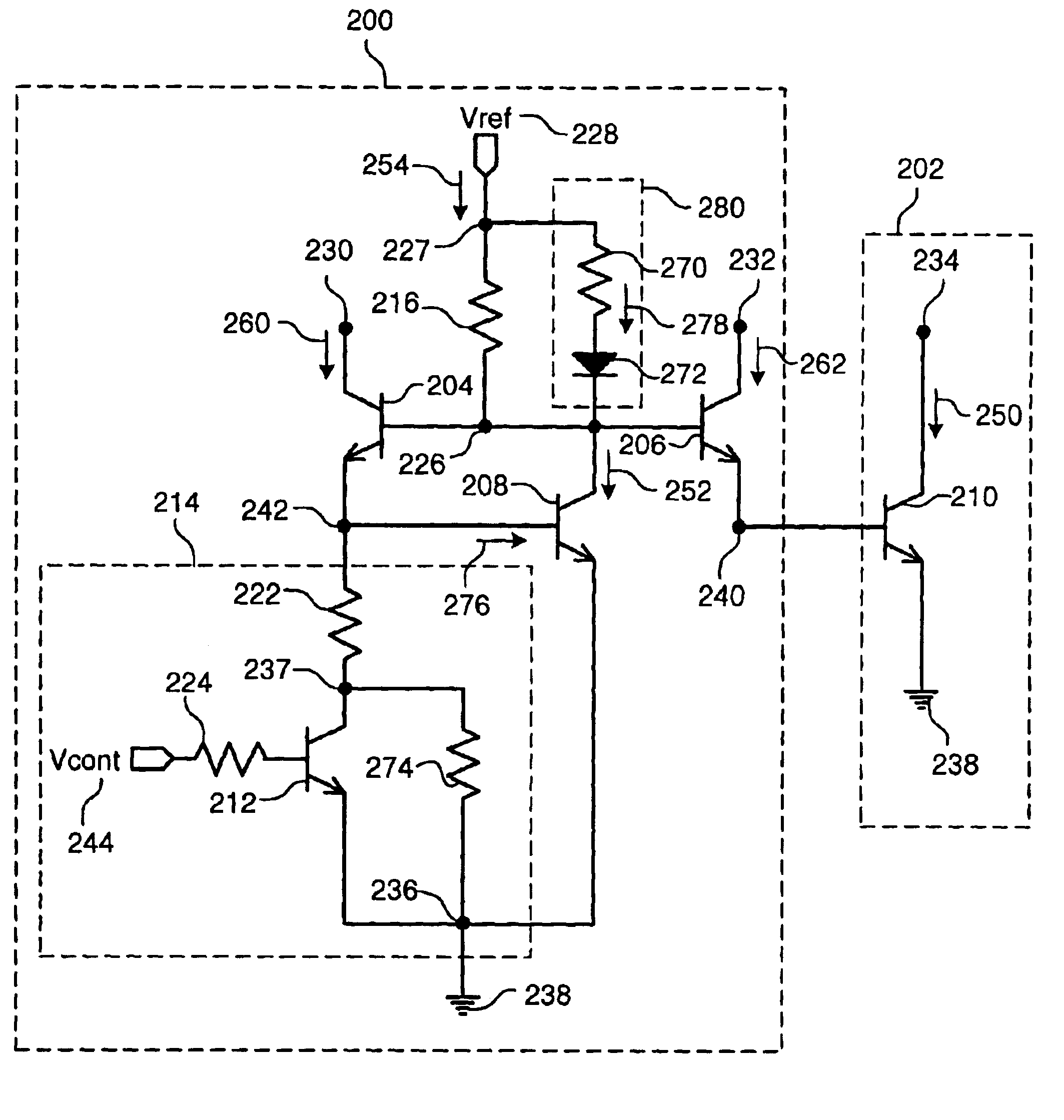
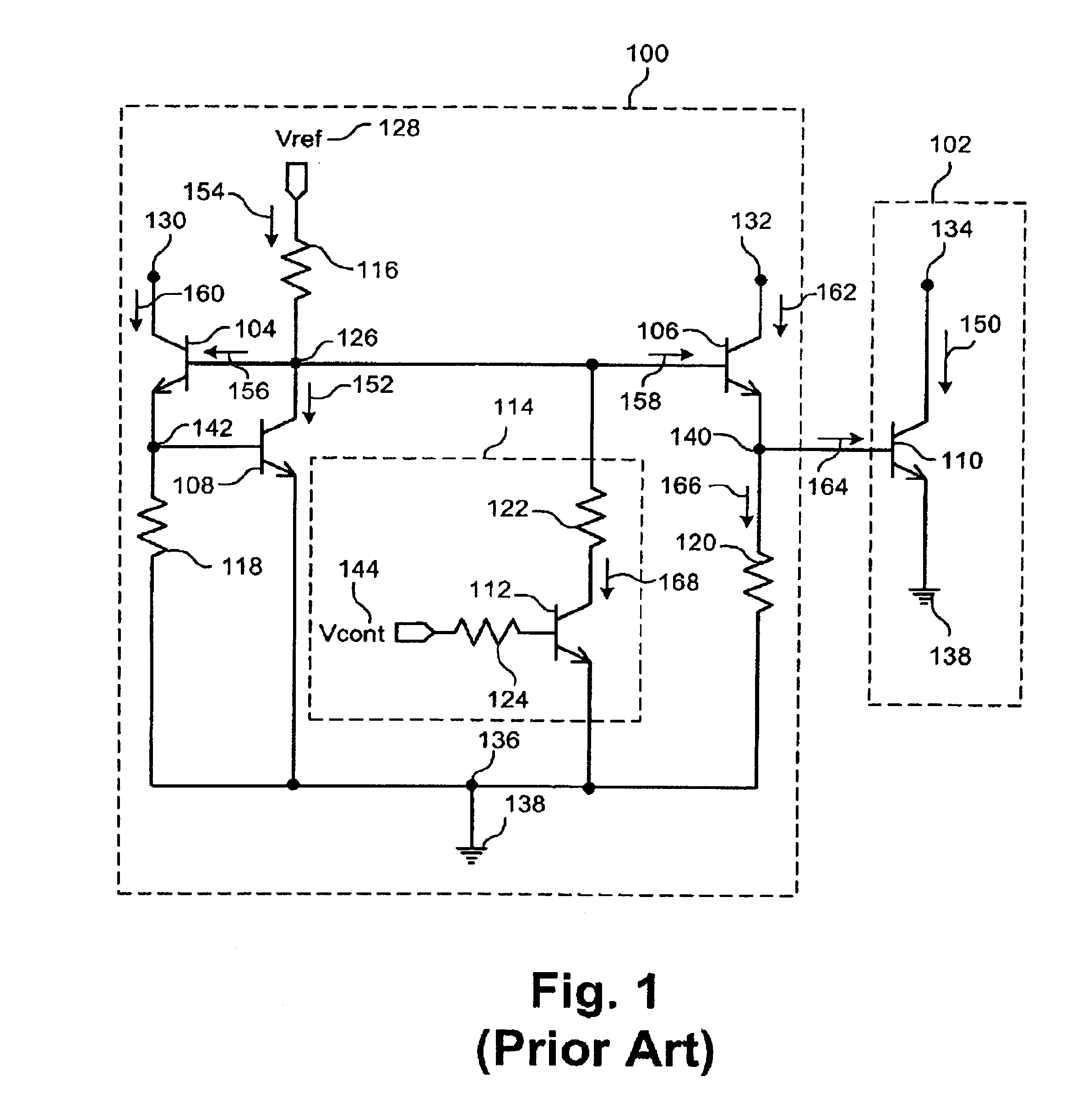
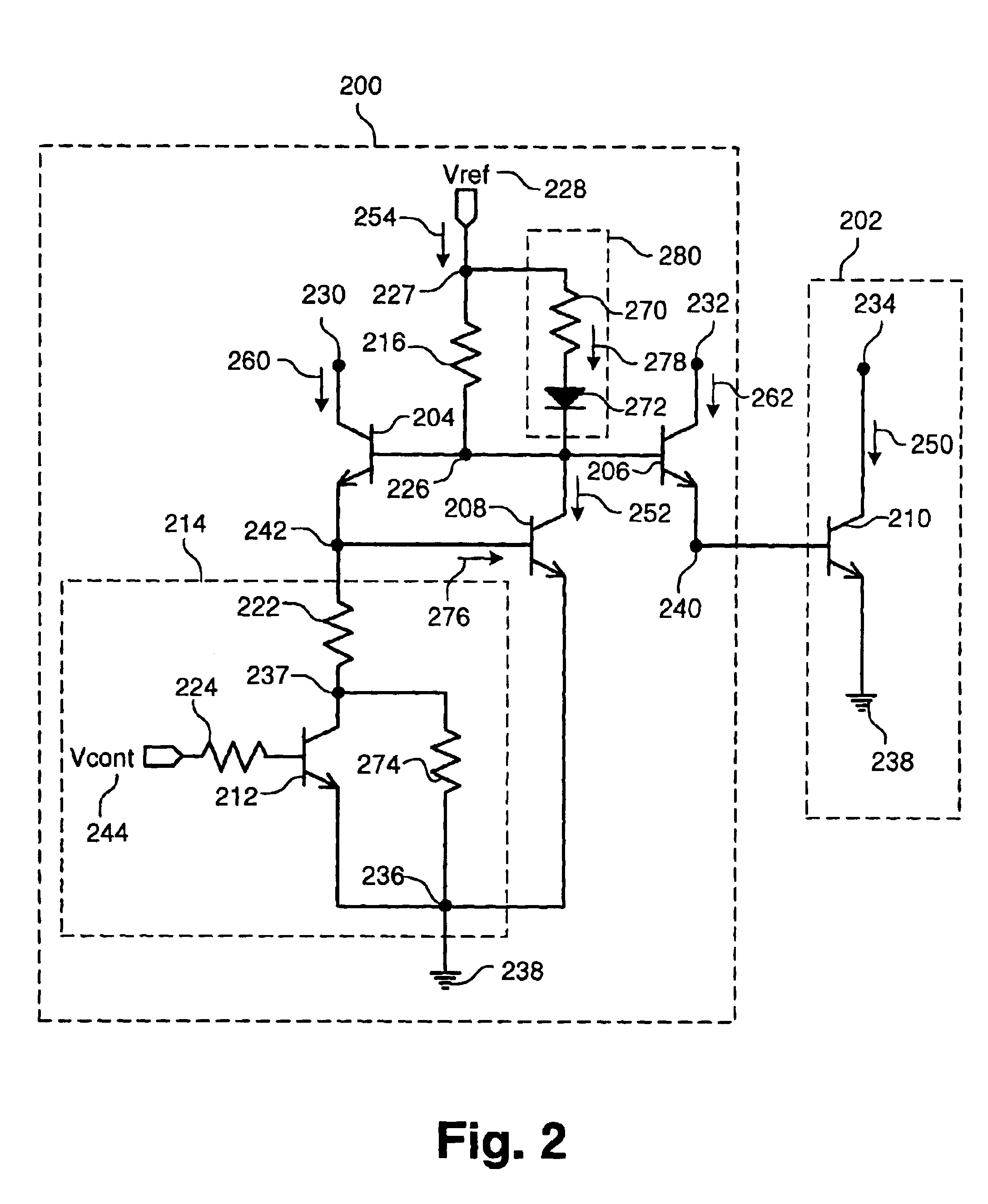
[0017]The present invention is directed to an area efficient, temperature-insensitive bias circuit for high-power amplifiers. The following description contains specific information pertaining to the implementation of the present invention. One skilled in the art will recognize that the present invention may be implemented in a manner different from that specifically discussed in the present application. Moreover, some of the specific details of the invention are not discussed in order not to obscure the invention. The specific details not described in the present application are within the knowledge of a person of ordinary skill in the art.

[0018]The drawings in the present application and their accompanying detailed description are directed to merely exemplary embodiments of the invention. To maintain brevity, other embodiments of the invention which use the principles of the present invention are not specifically described in the present application and are not specifically illust...


PUM


Abstract

An exemplary bias circuit is coupled to an amplifier. The bias circuit comprises a first bipolar transistor, a second bipolar transistor and a third bipolar transistor. The first bipolar transistor has a base connected to a first node, and the first node is connected to a reference voltage through a first resistor. The second bipolar transistor has a base connected to the first node. The third bipolar transistor has a collector connected to the first node and a base connected to an emitter of the first bipolar transistor at a second node. An emitter of the second bipolar transistor is connected to a base of a fourth bipolar transistor associated with the amplifier, and the second bipolar transistor does not have a resistor connected to the emitter of the second bipolar transistor.

Description

BACKGROUND OF THE INVENTION[0001]1. Field of the Invention[0002]The present invention is generally in the field of semiconductors. More specifically, the invention is in the field of semiconductor circuits.[0003]2. Related Art[0004]Amplifiers based on bipolar technology are widely used in a variety of applications, including wireless communication, such as radio frequency (“RF”) communication, for example. Bias circuits perform an important function by supplying the base bias current to the bipolar transistor for controlling the operation modes of the bipolar transistor.[0005]Currently known bias circuits for bipolar transistors, however, include a number of disadvantages. In general, known bias circuits consume large current and require a high reference voltage, or otherwise comprise very complex circuits which consume large die area, all of which are undesirable. Moreover, known bias circuits generally suffer from being temperature sensitive such that the quiescent current of the ...

Claims


Application Information

Patent Timeline
Patent Type & Authority Patents(United States)
IPC IPC(8): H03F3/04H01LH03F1/30
CPCH03F1/302H03F2200/18H03F2200/447H03F3/04H03F1/30
Inventor YANG, YOUNGOOCHOI, KEVINCHENG, NAI-SHUO
Owner SKYWORKS SOLUTIONS INC
Why Eureka
Try Eureka