1:N MEM switch module

a technology of mem switch and switch module, which is applied in the direction of waveguide type devices, electrical apparatus, electrostrictive/piezoelectric relays, etc., can solve the problems of circuits, increased power dissipation, cost, unit size and weight, etc., and achieves low insertion loss, reduced number of switches and die area required

Inactive Publication Date: 2007-01-02
TELEDYNE SCI & IMAGING
View PDF10 Cites 15 Cited by
  • Summary
  • Abstract
  • Description
  • Claims
  • Application Information

AI Technical Summary

Benefits of technology

[0009]A 1:N MEM switch module is presented which overcomes the problems noted above. Both the number of switches and the die area required are reduced when compared with conventional designs, while still providing low insertion loss and enabling operation at very high frequencies.
[0010]The module comprises N MEM switches fabricated on a common substrate. Each switch has an input contact and an output contact, and a movable contact which bridges the input and output contacts when the switch is actuated. A common signal input line on the substrate receives a signal to be switched. Each switch's input contact is connected to the common signal input line via a switch input line, and each output contact is connected to a respective signal output line. Each of the switch input lines has an associated inductance and effective capacitance, and each line is arranged such that its inductance is matched to its effective capacitance. This is done to reduce signal reflections which might arise due to the unterminated open stubs presented to the input signal by open switches; the inductance matching reduces reflections at the design frequency and thus the switch module's insertion loss. Matching is effected by, for example, using appropriately-sized open stub sections on the switch input lines in a manner to achieve equivalent performance for the different output paths.
[0011]The MEM switches are preferably located symmetrically about the terminus point of the common signal input line. This allows the switches to be tightly packed and the stub lengths to be kept small, which further reduces unwanted signal reflections. For example, a 1:4 MEM switch module preferably has four MEM switches arranged along four sides of a pentagon centered about the terminus point, with the common signal input line bisecting the fifth side of the pentagon en route to the terminus point. In this way, the die area required by the module is reduced. There may be applications, however, where different (non-symmetrical) configurations are preferred.

Problems solved by technology

However, there are several problems related to the use of solid-state switches, particularly at very high frequencies.
Additional gain must often be built into a system to compensate for the poor performance of the devices, increasing power dissipation, cost, and unit size and weight.
Providing switching with PIN diode circuits presents additional problems due to the parasitic capacitances inherently created by their use, which serve to limit the frequency range over which the circuit can operate.
Similar problems arise when the necessary switching is provided by off-chip switches, due to the parasitic capacitances that result from the presence of wire bonds.
This approach can also prove troublesome, however.
Switched signals can be subject to insertion losses due to inductance mismatch and signal reflection on the multiplexers' output lines.
This is particularly bad for an application such as the 2-bit phase shifter shown in FIG. 1, in which an incoming signal must pass through four MEM switches before reaching the output terminal.
Another drawback is that each multiplexer requires a considerable amount of die area.

Method used


Image

  • 1:N MEM switch module
  • 1:N MEM switch module
  • 1:N MEM switch module

Examples


Embodiment Construction

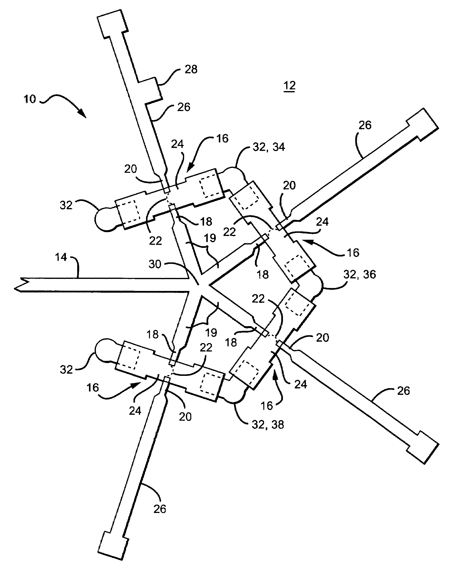
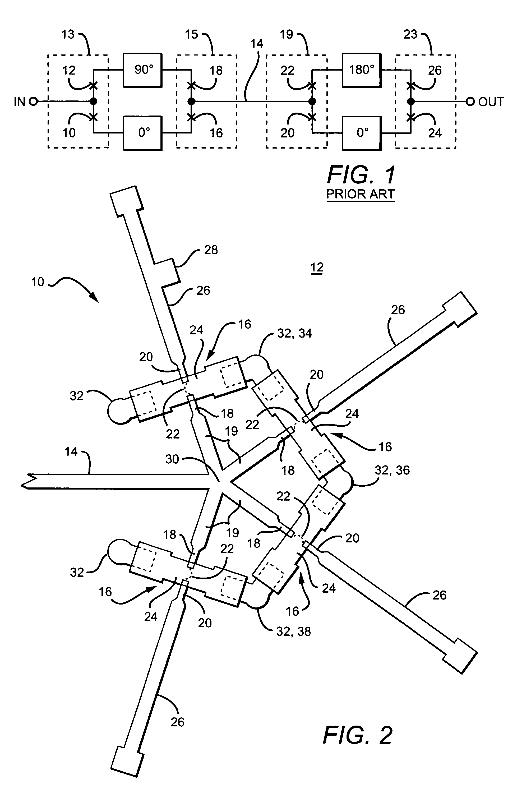
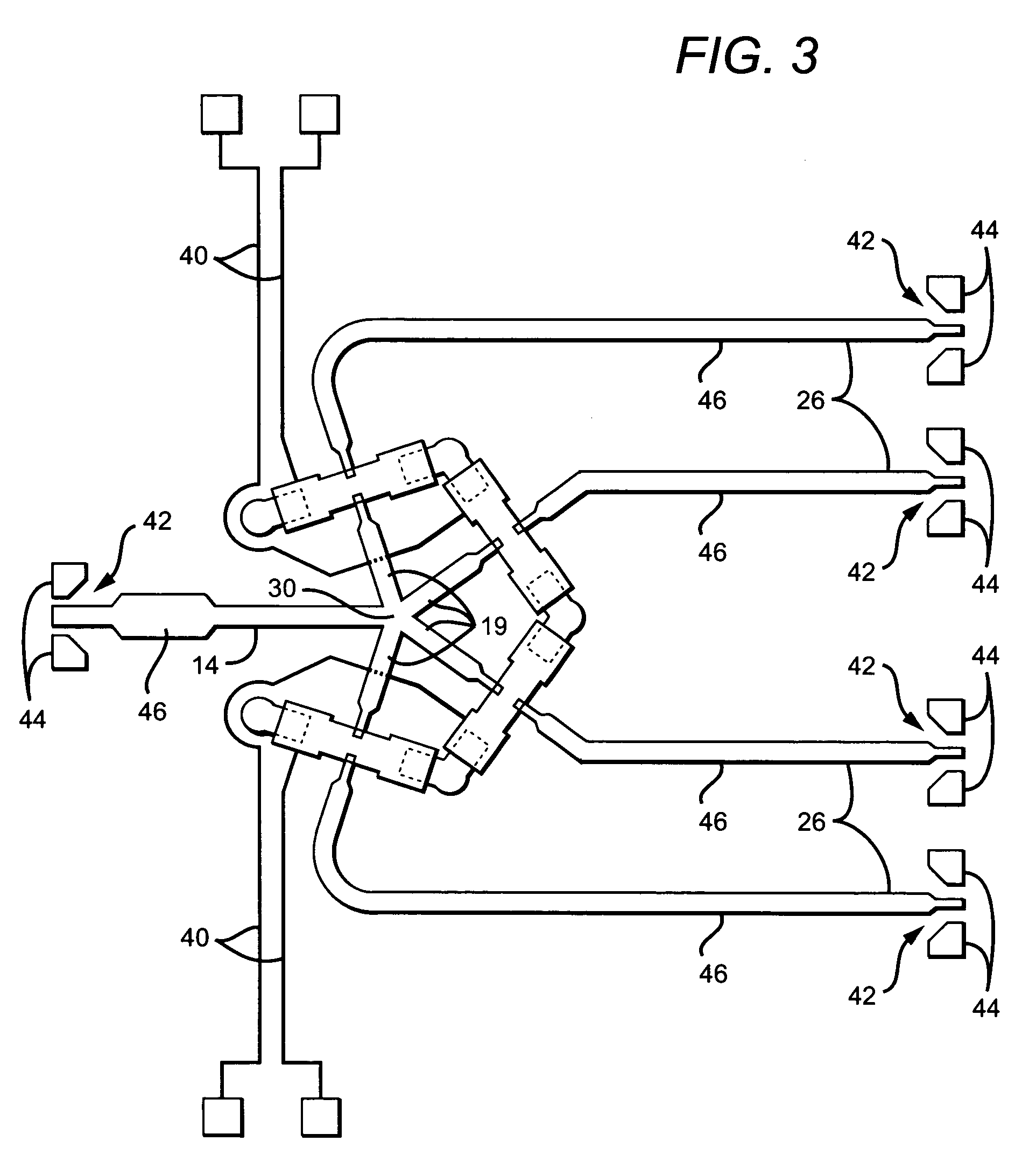
[0019]A plan view of a 1:N MEM switch module 10 in accordance with the present invention is shown in FIG. 2. The module's MEM switches and interconnecting traces are fabricated on a common substrate 12. The module comprises a common signal input line 14 which receives a signal to be switched, and N MEM switches 16; in the example shown, there are four MEM switches.

[0020]Each MEM switch in the module has an input contact 18 and an output contact 20 on substrate 12, with the two contacts separated by a gap 22. Each switch also includes a movable contact 24 which provides an electrically continuous path between the switch's input and output contacts when the switch is “actuated”. Each input contact 18 is connected to common signal input line 14 via a switch input line 19, and each output contact 20 is connected to a respective signal output line 26. While the MEM devices in this example are ohmic-contact switches which provide a conductive path upon closure, the invention can also be i...


PUM


Abstract

A 1:N MEM switch module comprises N MEM switches fabricated on a common substrate, each of which has input and output contacts and a movable contact which bridges the input and output contacts when the switch is actuated. The input contacts are connected to a common input node, and the output contacts are connected to respective output lines. Each output line has an associated inductance and effective capacitance, and is arranged such that its inductance is matched to its effective capacitance. The switches are preferably arranged symmetrically about the terminus point of the signal input line. A phase shifter employs at least two switch modules connected together with N transmission lines having different lengths, operated such that an input signal is routed via one of the transmission lines to effect a desired phase-shift.

Description

BACKGROUND OF THE INVENTION[0001]1. Field of the Invention[0002]This invention relates to the field of micro-electromechanical (MEM) devices, and particularly to MEM switches and their applications.[0003]2. Description of the Related Art[0004]Many circuits require a multiplexing function, in which an incoming signal is selectably switched to one of N output terminals. This is commonly accomplished with electromechanical or solid-state switches—typically field-effect transistors (FETs)—which are closed as necessary to provide the desired signal path.[0005]However, there are several problems related to the use of solid-state switches, particularly at very high frequencies. Integrated switches capable of handling such frequencies are typically implemented with gallium arsenide (GaAs) MESFETs or PIN diode circuits. At high signal frequencies (above about 900 MHz), these switching devices or circuits typically exhibit an insertion loss in the ON (closed) state of about 0.5 db. Additional...

Claims


Application Information

Patent Timeline
Patent Type & Authority Patents(United States)
IPC IPC(8): H01H51/22H01H59/00H01P1/12H01P1/18
CPCH01P1/184H01P1/127H01H59/0009H01H51/22H01P1/12H01P1/18
Inventor DENATALE, JEFFREY F.MIHAILOVICH, ROBERT E.HACKER, JONATHAN B.
Owner TELEDYNE SCI & IMAGING
Why Eureka
Try Eureka