Self-pinned in-stack bias structure for magnetoresistive read heads
a self-pinned bias and read head technology, applied in the field of magnetoresistive sensors, can solve the problems of difficult longitudinal bias stabilization of free (sense) layer using hard bias layers in the end regions to provide longitudinal bias
- Summary
- Abstract
- Description
- Claims
- Application Information
AI Technical Summary
Benefits of technology
Problems solved by technology
Method used
Image
Examples
first example
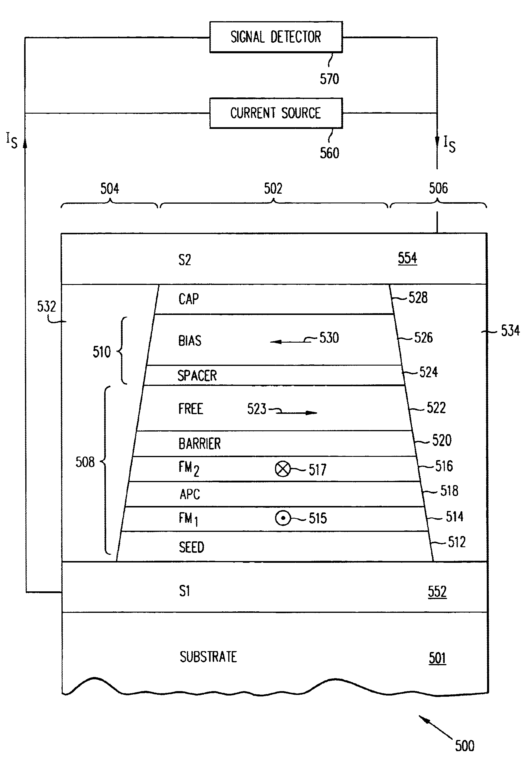
[0037]FIG. 5 depicts an air bearing surface (ABS) view, not to scale, of a MTJ sensor 500 having a self-pinned in-stack bias layer according to a first embodiment of the present invention. The MTJ sensor 500 comprises end regions 504 and 506 separated from each other by a central region 502. The substrate can be any suitable substrate including glass, semiconductor material, or a ceramic material such as alumina (Al2O3). The active region of the MTJ sensor comprises a MTJ stack 508 and a longitudinal bias stack 510 formed in the central region 502. The seed layer 512 is a layer deposited to modify the crystallographic texture or grain size of the subsequent layers. The MTJ stack 508 sequentially deposited over the seed layer comprises a first ferromagnetic layer (FM1) 514, an antiparallel coupling (APC) layer 518, a second ferromagnetic layer (FM2) 516, a tunnel barrier layer 520 and a ferromagnetic free layer 522. The APC layer 518 is formed of a nonmagnetic material, preferably ru...
second example
[0047]FIG. 6 shows an air bearing surface view (ABS) view, not to scale, of a CPP spin valve (SV) sensor 600 according to a second embodiment of the present invention. The SV sensor 600 differs from the MTJ sensor 500 depicted in FIG. 5 in having a CPP SV stack 608 in place of the MTJ stack 508. The active region of the SV sensor comprises the SV stack 608 and the longitudinal bias stack 510 formed in the central region 502. The SV stack 608 sequentially deposited over the seed layer 512 comprises a first ferromagnetic layer (FM1) 514, an antiparallel coupling (APC) layer 518, a second ferromagnetic layer (FM2) 516, a conductive spacer layer 620 and a ferromagnetic free layer 522. The conductive spacer layer 620, preferably formed of copper having a thickness of about 20 Å, replaces the insulating tunnel barrier layer 520 of the MTJ sensor 500 of the first example. The APC layer 518 is formed of a nonmagnetic material, preferably ruthenium (Ru), that allows the FM1 and FM2 layers 51...
PUM
| Property | Measurement | Unit |
|---|---|---|
| uniaxial anisotropy | aaaaa | aaaaa |
| thickness | aaaaa | aaaaa |
| resistance | aaaaa | aaaaa |
Abstract
Description
Claims
Application Information


