Semiconductor laser device

a laser device and semiconductor technology, applied in semiconductor lasers, lasers, laser details, etc., can solve problems such as the reduction of optical output due to the effect of slope efficiency and small reduction of optical outpu

Inactive Publication Date: 2005-09-20
MITSUBISHI ELECTRIC CORP
View PDF7 Cites 3 Cited by
  • Summary
  • Abstract
  • Description
  • Claims
  • Application Information

AI Technical Summary

Benefits of technology

[0018]The present invention has been devised to solve the above problems. It is, therefore, a primary object of the present invention to provide a semiconductor laser which exhibits only a small reduction in the optical output even when a large current flows and which has high slope efficiency and a near-field pattern not much different than that of conventional semiconductor lasers.
[0020]Therefore, light leakage is shifted toward a cladding layer side of the n-conductive type without changing the near-field pattern a great deal, resulting in reduced light absorption in the cladding-layer of the p-conductive type and enhanced slope efficiency.
[0021]Accordingly, it is possible to provide a semiconductor laser which has high optical output efficiency and exhibits only a small reduction in the optical output even when a large current flows and whose matching to optical fibers is not much different than that of conventional semiconductor lasers.

Problems solved by technology

However, the electric resistance of the p type semiconductor area generally tends to be higher than that of the n type semiconductor area, and reducing the carrier concentration of the p type semiconductor area further increases its electric resistance, entailing the problem of a reduction in the optical output due to heat produced when a large current flows, that is, the problem of roll-off.

Method used


Image

  • Semiconductor laser device
  • Semiconductor laser device
  • Semiconductor laser device

Examples


first embodiment

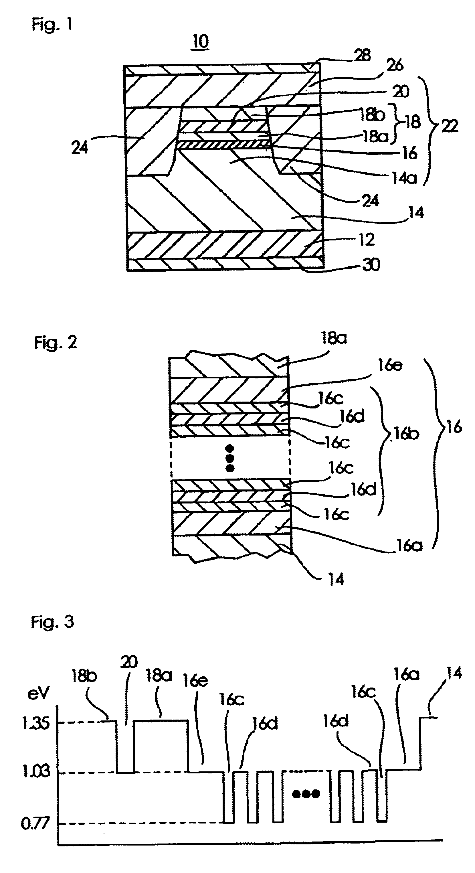
[0041]FIG. 1 is a cross-sectional view of a semiconductor laser according to a first embodiment of the present invention.

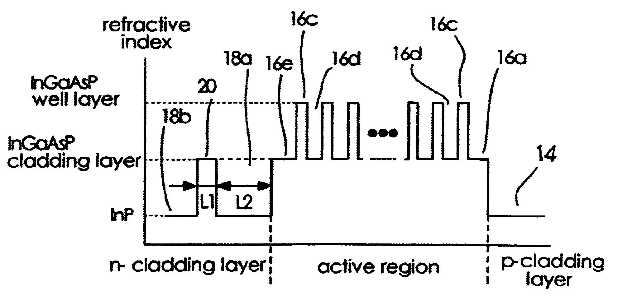
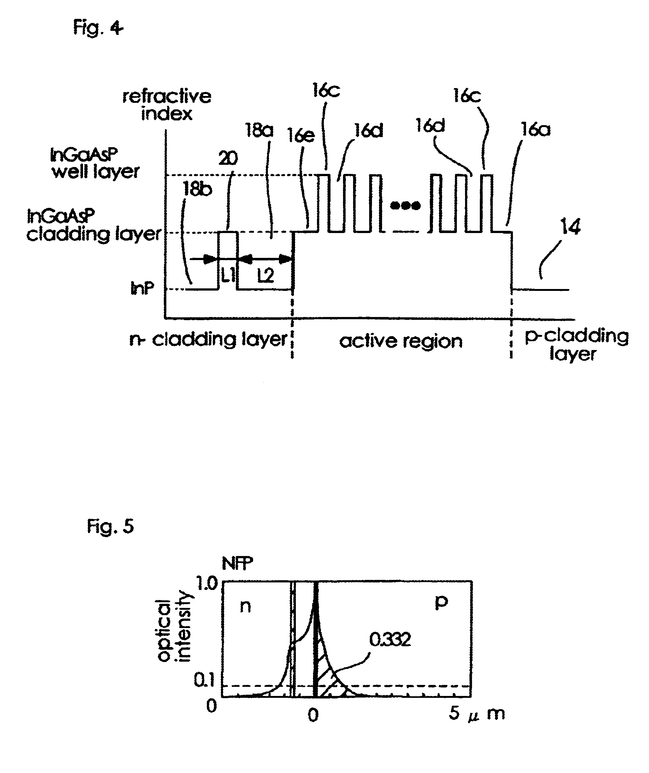
[0042]In the figure, reference numeral 10 denotes a semiconductor laser. In FIG. 1, the optical waveguide direction of the semiconductor laser 10 is perpendicular to the paper. Reference numeral 12 denotes a p-InP substrate used as the semiconductor substrate, and 14 denotes a p-InP cladding layer which is a first cladding layer disposed on the p-InP substrate 12. The p-InP cladding layer 14 has a bandgap energy of 1.35 eV, a layer thickness of 1,000 nm, and a carrier concentration of 1×1018 cm−1. Reference numeral 16 denotes an active region disposed on the p-InP cladding layer 14.

[0043]Reference numeral 18 denotes an n-InP cladding layer which is a second cladding layer disposed on the active region 16. According to the present embodiment, the n-InP cladding layer 18 comprises two layers: an n-InP cladding layer 18a adjacent the active region 16; and an n-InP cl...

second embodiment

[0090]FIG. 8 is a cross-sectional view of a semiconductor laser according to a second embodiment of the present invention.

[0091]In the figure, reference numeral 40 denotes a semiconductor laser. In FIG. 8, the optical waveguide direction of the semiconductor laser 40 is perpendicular to the paper. Reference numeral 42 denotes a p-AlGaInAs cladding layer used as the semiconductor layer.

[0092]Employing a p-InP substrate 12, the semiconductor laser 40 is configured much in the same way as the semiconductor laser 10 of the first embodiment. However, whereas the semiconductor laser 10 is configured such that the n-InGaAsP cladding layer 20 having a refractive index higher than that of the n-InP cladding layer 18 is inserted into the n-InP cladding layer 18, the semiconductor laser 40 is configured such that a p-AlGaInAs cladding layer having a refractive index lower than that of the p-InP cladding layer 14 is inserted into the p-InP cladding layer 14.

[0093]In the semiconductor laser 40, ...

third embodiment

[0112]FIG. 11 is a cross-sectional view of a semiconductor laser according to a third embodiment of the present invention.

[0113]In the figure, reference numeral 50 denotes a semiconductor laser. In FIG. 11, the optical waveguide direction of the semiconductor laser 50 is perpendicular to the paper.

[0114]Reference numeral 52 denotes an n-InP substrate used as the semiconductor substrate. The n-InP substrate 52 has disposed thereon the n-InP cladding layer 18b which in turn has the n-InGaAsP cladding layer 20 disposed thereon. Furthermore, the n-InP cladding layer 18a is disposed on the n-InGaAsP cladding layer 20. The n-InP cladding layers 18a and 18b collectively constitute the n-InP cladding layer 18, which is a first cladding layer.

[0115]In addition, the active region 16 is disposed on the n-InP cladding layer 18a, and the p-InP cladding layer 14, which is a second cladding layer, is disposed on the active layer 16.

[0116]The p-InP cladding layer 14, the active region 16, the n-InP...


PUM


Abstract

A semiconductor laser device includes a p-InP cladding layer, an active region, a first n-InP cladding layer, a second n-InP cladding layer, and an n-InGaAsP cladding layer with a thickness between 0.05 μm and 0.3 μm, sandwiched by the first and second n-laP cladding layers and laminated at a position closer to the active region than a position at which optical intensity of a near-field pattern of laser light emitted from the active region becomes substantially zero. The semiconductor laser device exhibits a small reduction in the optical output even when a large current flows, and has a high slope efficiency without changing the near-field pattern a great deal.

Description

BACKGROUND OF THE INVENTION[0001]1. Field of the Invention[0002]The present invention relates to a semiconductor laser device used for optical communications and, more particularly, to a semiconductor laser device having an asymmetrical optical intensity distribution.[0003]2. Description of the Related Art[0004]With the spread of public networks using optical fibers, there is an increasing need to transmit a large amount of information at low cost. To meet such a need, the public networks must be improved at low cost to increase the amount of information that can be transmitted. This requires the development of a semiconductor laser device which has good optical matching to the existing optical fiber networks and high optical output efficiency.[0005]FIG. 15 is a cross-sectional view of a conventional semiconductor laser.[0006]In the figure, reference numeral 200 denotes a semiconductor laser; 202 a p conductivity type InP substrate (“p conductivity type” and “n conductivity type” ar...

Claims


Application Information

Patent Timeline
Patent Type & Authority Patents(United States)
IPC IPC(8): H01S5/30H01S5/34H01S5/20H01S5/00H01S5/227H01S5/343
CPCB82Y20/00H01S5/20H01S5/227H01S5/2004H01S5/34373H01S5/305H01S5/34306H01S5/30
Inventor NAKAYAMA, TAKESHI
Owner MITSUBISHI ELECTRIC CORP
Why Eureka
Try Eureka