Methods and apparatus for the optimization of photo resist etching in a plasma processing system

Active Publication Date: 2005-09-27
LAM RES CORP
View PDF6 Cites 2 Cited by
  • Summary
  • Abstract
  • Description
  • Claims
  • Application Information

AI Technical Summary

Benefits of technology

[0016]The invention relates, in one embodiment, in a plasma processing system, to a method of minimizing the differences in an etch rate of a photo resist material in different regions of a substrate. The method includes introducing the substrate having in sequential order thereon, an underlying layer and the photo-resist layer. The method also includes flowing the etchant gas mixture into a plasma reactor of the plasma processing system, the etchant gas mixture comprising a flow of a fluorine containing gas between about 0.1% and about 10% of the etchant gas mixture. The method further includes striking a plasma from the gas mixture; etching the photo-resist layer with the plasma; and, removing the substrate from the plasma reactor.
[0017]The invention relates, in

Problems solved by technology

For example, when the photo resist is added as a blanket and then etched back, such as when trenches are being formed for dual-damascene structures, it is fairly difficult to apply a perfectly uniform layer of photo resist.
Subsequently, non-uniform photo resist profiles among the trenches may be created, potentially causing qual

Method used


Image

  • Methods and apparatus for the optimization of photo resist etching in a plasma processing system
  • Methods and apparatus for the optimization of photo resist etching in a plasma processing system
  • Methods and apparatus for the optimization of photo resist etching in a plasma processing system

Examples


Example

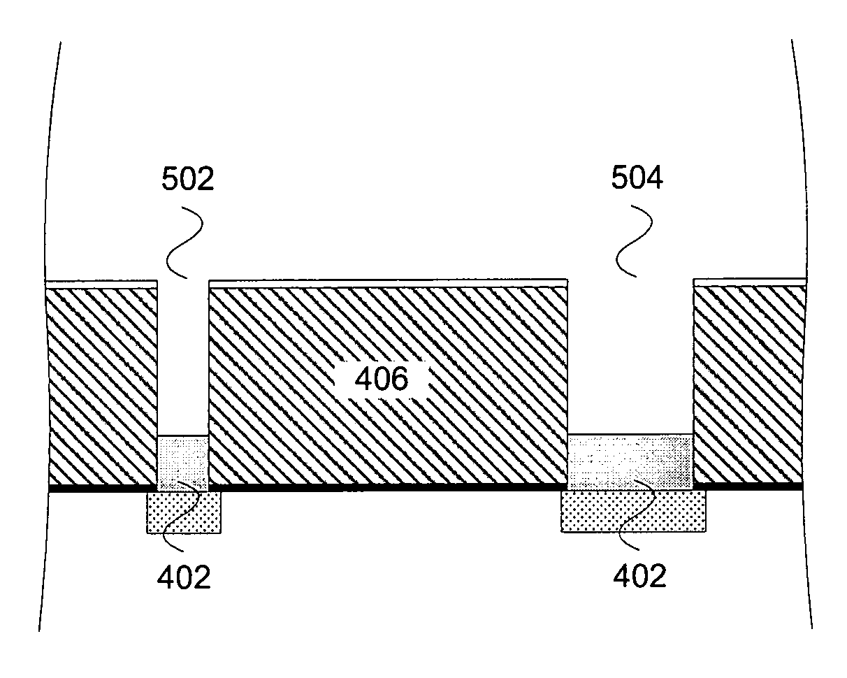
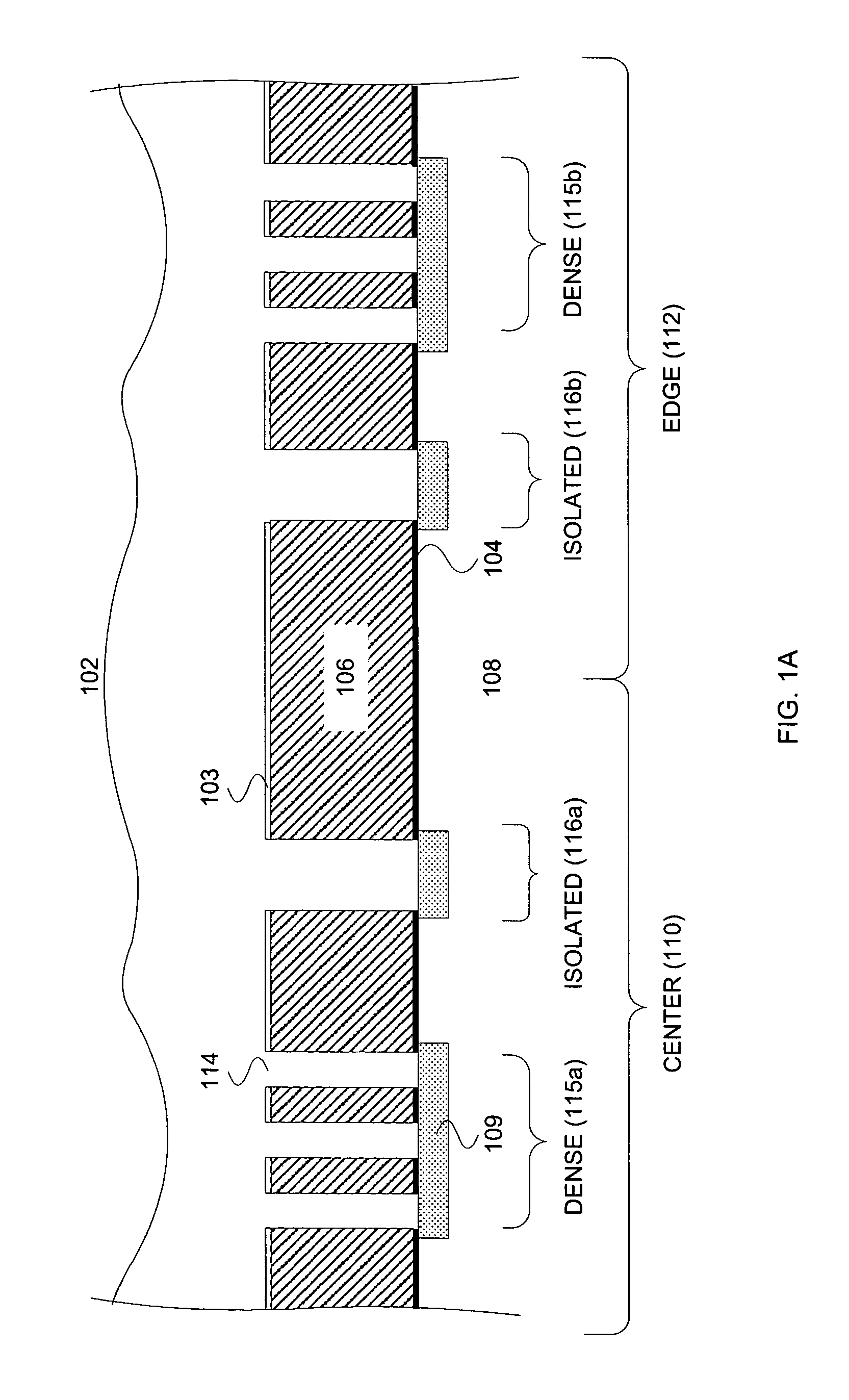
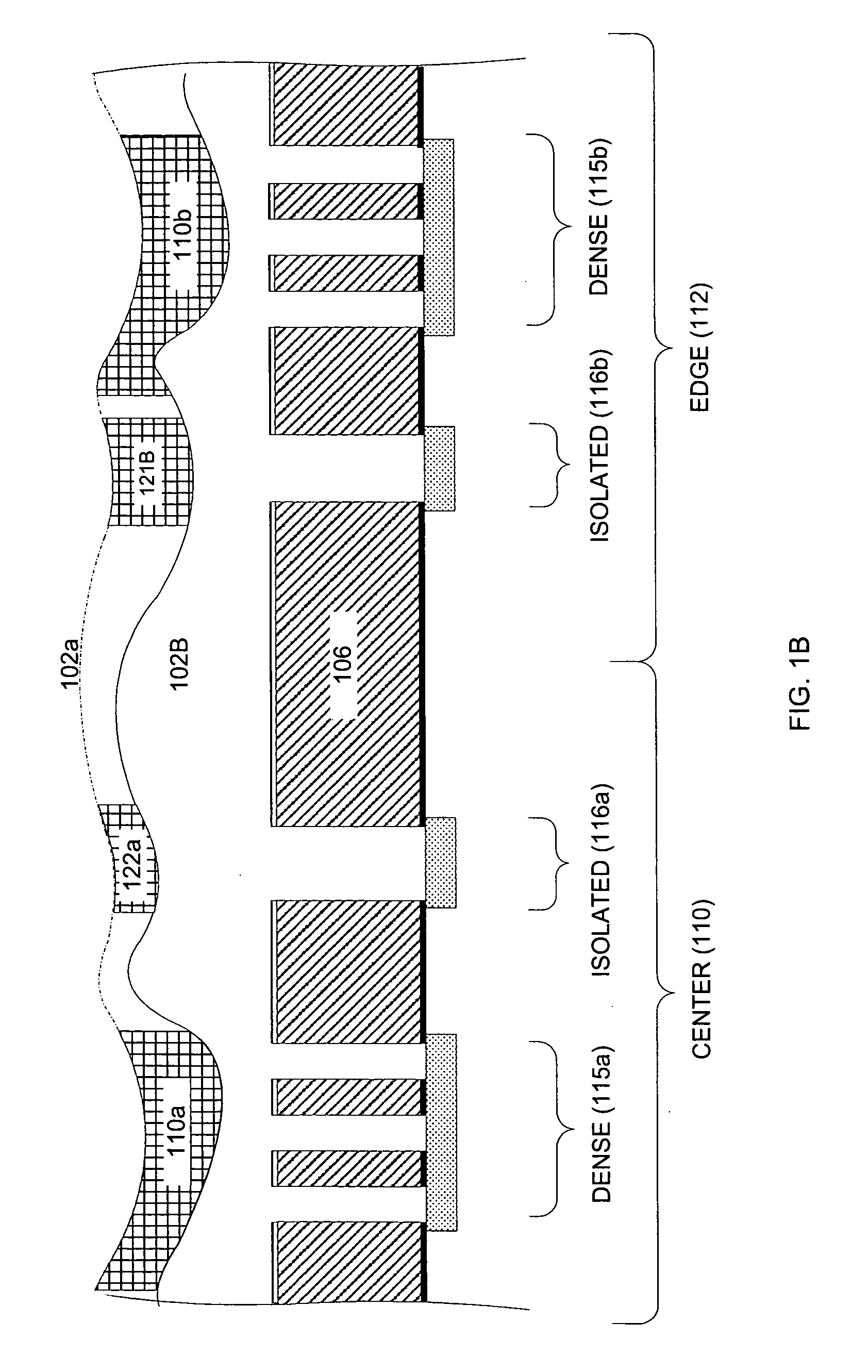
[0025]The present invention will now be described in detail with reference to a few preferred embodiments thereof as illustrated in the accompanying drawings. In the following description, numerous specific details are set forth in order to provide a thorough understanding of the present invention. It will be apparent, however, to one skilled in the art, that the present invention may be practiced without some or all of these specific details. In other instances, well known process steps and / or structures have not been described in detail in order to not unnecessarily obscure the present invention.

[0026]In the following paragraphs, approximate ranges believed to be suitable for performing the inventive method of improving process results through the introduction of additional gasses into a plasma processing chamber are disclosed. Although the suitable ranges are disclosed herein below in connection with an Exelan™ HPT plasma processing system, these ranges should serve as guidelines...


PUM


Abstract

In a plasma processing system, a method of minimizing the differences in an etch rate of a photo resist material in different regions of a substrate is disclosed. The method includes introducing the substrate having in sequential order thereon, an underlying layer and the photo-resist layer. The method also includes flowing the etchant gas mixture into a plasma reactor of the plasma processing system, the etchant gas mixture comprising a flow of a fluorine containing gas between about 0.1% and about 10% of the etchant gas mixture. The method further includes striking a plasma from the gas mixture; etching the photo-resist layer with the plasma; and, removing the substrate from the plasma reactor.

Description

BACKGROUND OF THE INVENTION[0001]The present invention relates in general to substrate manufacturing technologies and in particular to methods and apparatus for the optimization of photo resist.[0002]In the processing of a substrate, e.g., a semiconductor substrate or a glass panel such as one used in flat panel display manufacturing, plasma is often employed. As part of the processing of a substrate for example, the substrate is divided into a plurality of dies, or rectangular areas, each of which will become an integrated circuit. The substrate is then processed in a series of steps in which materials are selectively removed (etching) and deposited (deposition) in order to form electrical components thereon.[0003]In an exemplary plasma process, a substrate is coated with a thin film of hardened emulsion (i.e., such as a photo resist mask) prior to etching. Areas of the hardened emulsion are then selectively removed, causing parts of the underlying layer to become exposed. The subs...

Claims


Application Information

Patent Timeline
IPC IPC(8): H01L21/02H01L21/302H01L21/461H01L21/311
CPCH01L21/31138H01L21/31144
Inventor CHENG, YUZHU, HELENPHORAY, VINAY V.XIAO, HANZHONGLOEWENHARDT, PETER K.
Owner LAM RES CORP
Why Eureka
Try Eureka