Versatile system for controlling driver signal timing

a technology of driver signal and timing, applied in the direction of pulse generator, pulse technique, electronic switching, etc., can solve the problems of affecting the fall time and propagation delay, circuit generation generates numerous challenges to the semiconductor manufacturing process, and certain issues, etc., to achieve reliable device performance, easy, efficient and cost-effective

Active Publication Date: 2005-10-04
TEXAS INSTR INC
View PDF3 Cites 6 Cited by
  • Summary
  • Abstract
  • Description
  • Claims
  • Application Information

AI Technical Summary

Benefits of technology

[0014]The present invention provides a versatile system of methods and structures that accurately control drive signal fall times and propagation delay through a driver circuitry segment in a constrained and efficient manner. The system of the present invention provides driver circuitry that satisfies stringent timing requirements while delivering reliable device performance in an easy, efficient and cost-effective manner—overcoming certain limitations associated with conventional approaches.
[0015]Specifically, the present invention provides a low impedance output discharge system that channels discharge current to an operational load attached thereto. The system of the present invention provides a discharge structure and an output structure fabricated from homogeneous semiconductor material types. The system of the present invention provides a pre-drive system comprising elements for selectively controlling signal fall time for the output structure. As a result, system performance and reliability is optimized with minimal augmentation of semiconductor device layout and fabrication.

Problems solved by technology

The increased packing density of the integrated circuit generates numerous challenges to the semiconductor manufacturing process.
Unfortunately, however, there are a large number of variables in semiconductor device manufacturing that can affect any given performance parameter.
If, however, rise and fall times of a drive signal originating from segment 106 are particularly critical, then certain issues may arise in system 100.
Signal fall times and propagation delays are typically affected to a greater extent, since—generally—device discharge phenomena tend to be more problematic than device charging phenomena.
This can present a significant problem, especially in a number of modern end-equipment applications where increasingly faster data transfer and performance rates are demanded.
Unfortunately, a number of these conventional systems channel that discharge through the semiconductor device itself, not load 128.
This increases power dissipation in device 108.
Furthermore, circuitry and routing for such a purpose can add considerable design and fabrication overhead to a semiconductor device.
Such an approach usually results in increased costs, decreased reliability, or yield problems.
As a result, inexact device matching can, and often does, occur.
This can shift propagation delays on a device-to-device, wafer-to-wafer or lot-to-lot basis—profoundly degrading overall device reliability.
Furthermore, such approaches can create undesirable circuitry behaviors—such as overdriving the output into cutoff, or loss of fall time control.
Overdriving the output into cutoff can cause an output fall time to have a large dv / dt during a portion of the fall time.
When a device is non-compliant, it is scrapped—degrading yield and increasing costs.

Method used


Image

  • Versatile system for controlling driver signal timing
  • Versatile system for controlling driver signal timing

Examples


Embodiment Construction

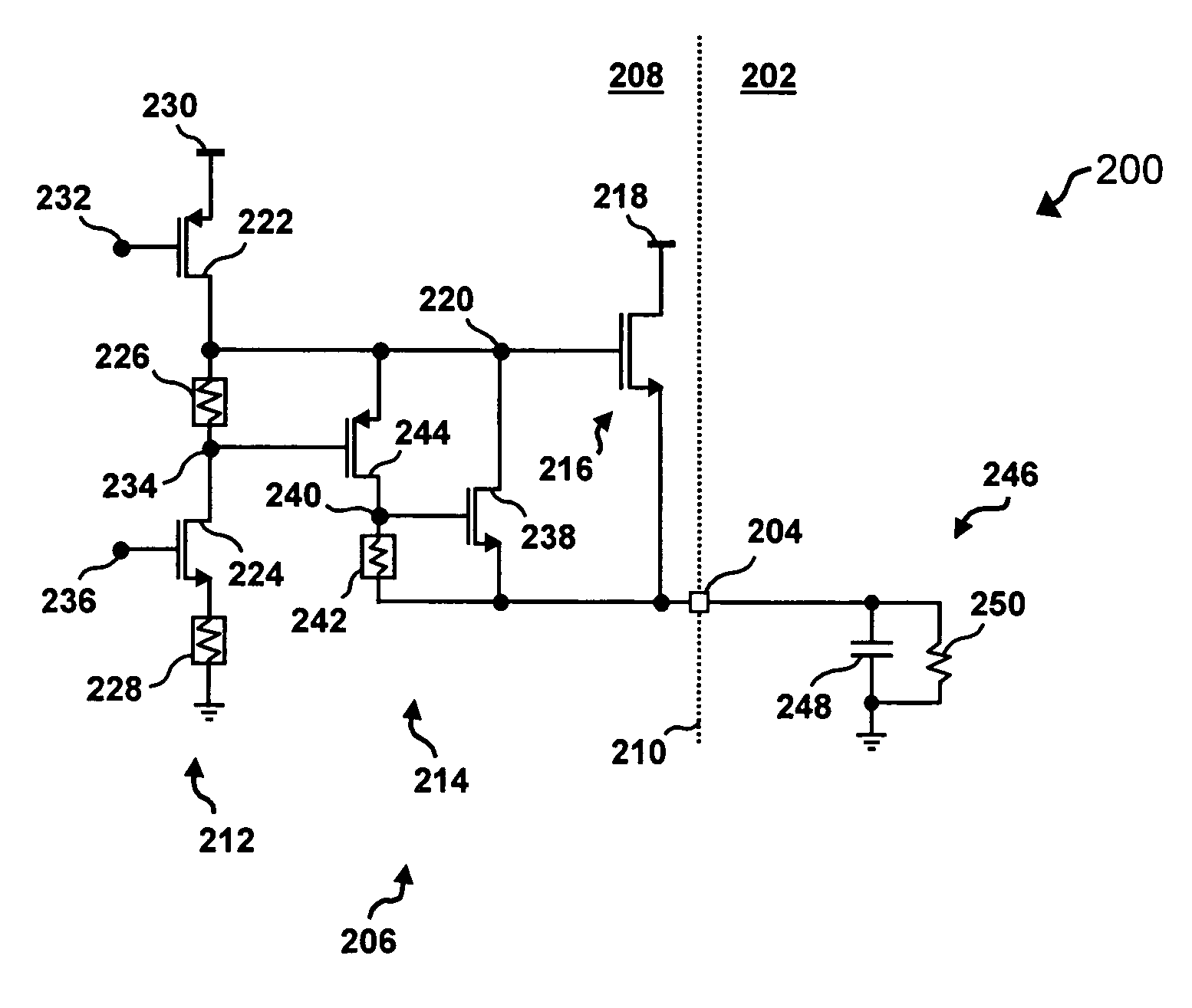
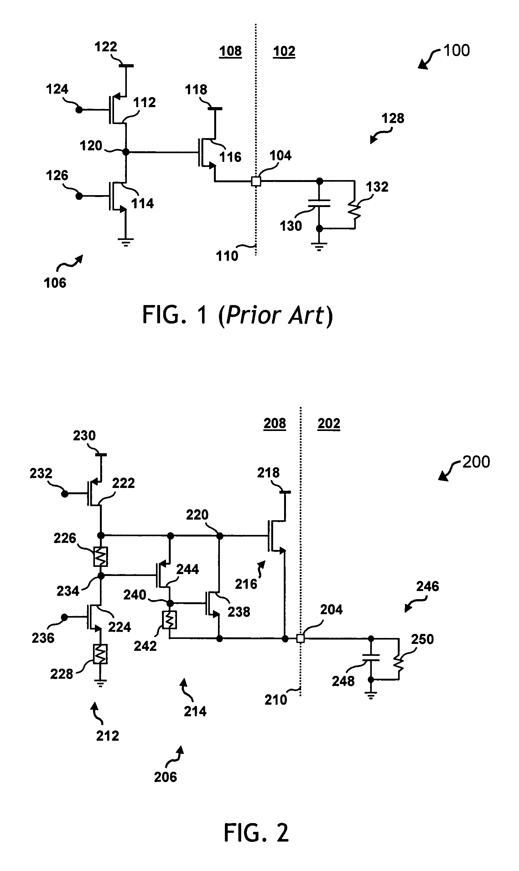
[0023]While the making and using of various embodiments of the present invention are discussed in detail below, it should be appreciated that the present invention provides many applicable inventive concepts, which can be embodied in a wide variety of specific contexts. The invention will now be described in conjunction with high side driver circuitry utilized in an end equipment system that requires minimal propagation delays, controlled rise and fall times, and variable driver supply voltages. The specific embodiments discussed herein are, however, merely illustrative of specific ways to make and use the invention and do not limit the scope of the invention.

[0024]The system of the present invention provides a versatile system, comprising various methods and structures, providing accurate control of drive signal fall time and propagation delay through a driver circuitry segment in a constrained and efficient manner. The present invention provides a low impedance discharge structure...


PUM


Abstract

The present invention provides a system (200) for controlling drive signal timing parameters of an output driver circuit (206). The present invention defines a driver circuit having an output interface (204), and a first transistor (222) coupled to a first voltage supply (230), a first control signal (232), and a first node (220). The circuit also has a first resistive element, coupled between the first node and a second node (234). A second resistive element (228) is coupled to ground. A second transistor (224) is coupled to the second node, to a second control signal (236), and the second resistive element. The circuit has a third transistor (244), coupled to the first and second nodes, and to a third node (240). A third resistive element (242) is coupled between the third node and the output interface. A fourth transistor (238) is coupled to the first and third nodes, and to the output interface. The circuit also has a fifth transistor (216), coupled to a second voltage supply (218), to the first node, and to the output interface.

Description

TECHNICAL FIELD OF THE INVENTION[0001]The present invention relates generally to the field of semiconductor devices and, more particularly, to apparatus and methods for controlling drive signal timing in driver circuitry.BACKGROUND OF THE INVENTION[0002]The continual demand for enhanced integrated circuit performance has resulted in, among other things, a dramatic reduction of semiconductor device geometries, and continual efforts to optimize the performance of every substructure within any semiconductor device. A number of improvements and innovations in fabrication processes, material composition, and layout of the active circuit levels of a semiconductor device have resulted in very high-density circuit designs. Increasingly dense circuit design has not only improved a number of performance characteristics, it has also increased the importance of, and attention to, semiconductor device properties and behaviors.[0003]The increased packing density of the integrated circuit generate...

Claims


Application Information

Patent Timeline
Patent Type & Authority Patents(United States)
IPC IPC(8): H03B1/00H03K17/0412
CPCH03K17/04123
Inventor RAHMAN, MD ABIDURGROSE, WILLIAM E.SMITH, BRETT E.
Owner TEXAS INSTR INC
Why Eureka
Try Eureka