Magnetic sensing element having second antiferromagnetic layer on edge sections and rear end of a middle section of free magnetic layer

Inactive Publication Date: 2005-10-04
TDK CORPARATION
View PDF5 Cites 12 Cited by
  • Summary
  • Abstract
  • Description
  • Claims
  • Application Information

AI Technical Summary

Benefits of technology

[0020]The present invention was made to overcome the aforementioned problems. Accordingly, it is an object of the present invention to provide a magnetic sensing element having small hysteresis and an excellent playback characteristic, in which the arrangement position of the second antiferromagnetic layer is in particular optimized, and turbulence in the magnetization of a free magnetic layer due to a sense current magnetic field is thereby alleviated.

Problems solved by technology

Since the CPP type magnetic sensing element has a small element resistance, a large playback output cannot be attained unless the sense current density is increased.
Consequently, hysteresis is exhibited, and degradation of the playback characteristic is brought about.
However, since the aforementioned vertical bias magnetic field becomes excessively strong, the magnetization of the aforementioned free magnetic layer 5 becomes likely to be pinned.
Therefore, highly sensitive magnetic reversal is not brought about with respect to an external magnetic field, and a problem of degradation of the playback characteristic occurs.

Method used


Image

  • Magnetic sensing element having second antiferromagnetic layer on edge sections and rear end of a middle section of free magnetic layer
  • Magnetic sensing element having second antiferromagnetic layer on edge sections and rear end of a middle section of free magnetic layer
  • Magnetic sensing element having second antiferromagnetic layer on edge sections and rear end of a middle section of free magnetic layer

Examples


examples

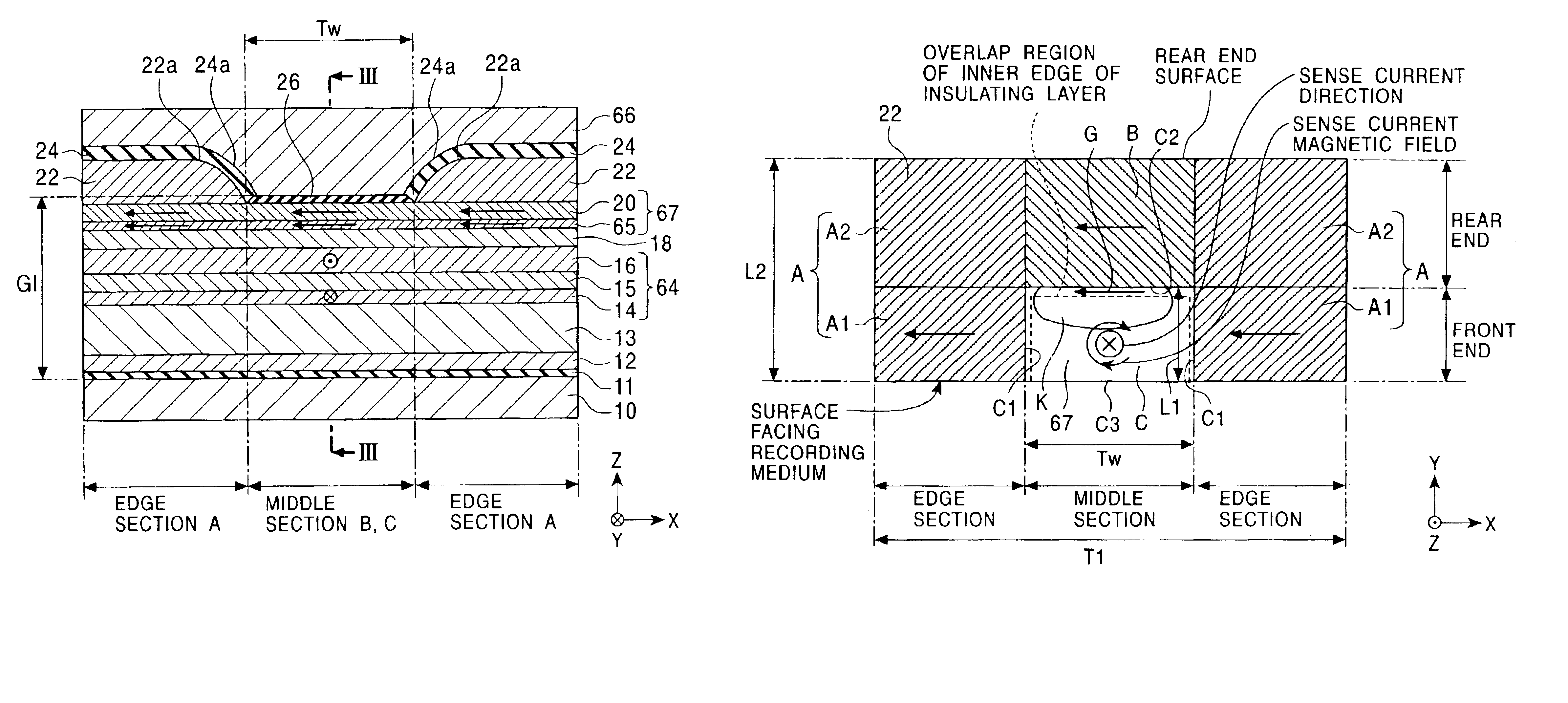
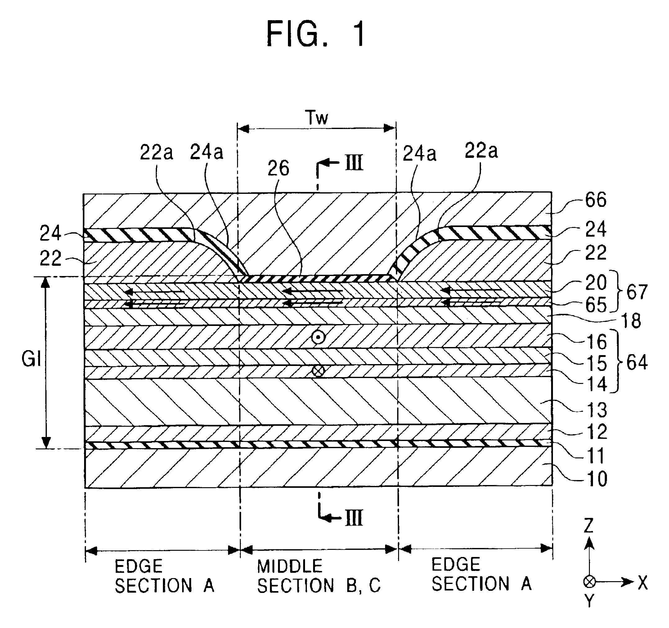
[0250]A magnetic sensing element for an experiment having a film configuration similar to that of the magnetic sensing element shown in FIG. 1 was prepared, and R-H curves (may be referred to as QST curves) were drawn using this magnetic sensing element.

[0251]The film configuration of the magnetic sensing element used for the experiment will be described below with reference to FIG. 1. In the magnetic sensing element for the experiment, a lower electrode made of Cr / Ta was used instead of the lower shield layer 10, and a seed layer 12 made of (Ni0.8Fe0.2)60 at %Cr40 at % (60 angstroms) was formed on this lower electrode. A first antiferromagnetic layer made of PtMn (150 angstroms), a pinned magnetic layer 64 composed of a laminated ferrimagnetic structure of Co90 at %Fe10 at % (20 angstroms) / Ru (20 angstroms) / Co90 at %Fe10 at % (30 angstroms), a non-magnetic material layer 18 made of Cu (25 angstroms) land a free magnetic layer 67 composed of a single-layer structure of CoFe (50 angs...


PUM


Abstract

A CPP type magnetic sensing element capable of properly performing magnetization control of a free magnetic layer and having small hysteresis and an excellent playback characteristic, as well as a manufacturing method therefor, are provided. Second antiferromagnetic layers are provided not only on both edge sections of the free magnetic layer, but also on the middle rear end. In the height-side edge of the middle front end of the aforementioned free magnetic layer, a sense current magnetic field in the direction opposite to the magnetization direction of the aforementioned free magnetic layer is cancelled by a bias magnetic field from the second antiferromagnetic layer provided on the middle rear end. Consequently, an influence of the aforementioned sense current magnetic field can be reduced, turbulence in the magnetization of the aforementioned free magnetic layer can be made smaller than ever, and a magnetic sensing element having small hysteresis can be manufactured.

Description

[0001]This application claims the benefit of priority to Japanese Patent Application 2002-077749, filed on Mar. 20, 2002.BACKGROUND OF THE INVENTION[0002]1. Field of the Invention[0003]The present invention relates to a CPP (current perpendicular to the plane) type magnetic sensing element. In particular, the present invention relates to a magnetic sensing element capable of properly performing magnetization control of a free magnetic layer.[0004]2. Description of the Related Art[0005]FIG. 31 is a partial sectional view of the structure of a conventional magnetic sensing element, viewed from the side of the surface facing a recording medium.[0006]Reference numeral 1 denotes a lower electrode, and a first antiferromagnetic layer 2 made of PtMn or the like is arranged on the aforementioned lower electrode 1. A pinned magnetic layer 8 formed from CoFe or the like is further arranged on the aforementioned first antiferromagnetic layer 2, a non-magnetic material layer 4 formed from Cu or...

Claims


Application Information

Patent Timeline
IPC IPC(8): G01R33/06G01R33/09G11B5/39G11B5/00H01L43/08
CPCB82Y10/00B82Y25/00G01R33/093G11B5/3903G11B5/3909G11B2005/0016
Inventor HASEGAWA, NAOYA
Owner TDK CORPARATION
Why Eureka
Try Eureka