Light modulating device and exposure apparatus using the same

a light modulating device and light modulating technology, applied in the direction of shades, point-like light sources, lenses, etc., can solve the problems of limiting a kind of light source, generating disadvantages in high-speed response, and not getting practical useful resolution, so as to improve the usability of light and improve the resolution

Inactive Publication Date: 2005-10-11
FUJIFILM HLDG CORP +1
View PDF6 Cites 12 Cited by
  • Summary
  • Abstract
  • Description
  • Claims
  • Application Information

AI Technical Summary

Benefits of technology

[0015]In view of the foregoing circumstance, it is a first object of the present invention to obtain the light modulating device, in which usability of the light is improved and resolution is increased in the projection exposure, and the exposure apparatus using the same.
[0016]Further, it is a second object of the invention to obtain the transmission two-dimensional light modulating device, in which the high-speed response is realized, the two-dimensionability is easily achieved, low-voltage drive can be realized, in addition, the optical system is simple, and the low-cost is achieved, and the exposure apparatus using the same.
[0018]Due to the above-described structure of the invention, condensing effect of the lens array improves the usability of the light and the resolution is improved in the projection exposure by forming the substantial light-modulating-element size smaller than the light-modulating-element region. By using the micro electro-mechanical transmission two-dimensional light modulating device, the high-speed response can be achieved, two-dimensionability can be easily realized, the low-voltage drive can be realized, the optical system can be simplified, and low-cost can be achieved. Further, since the micro electro-mechanical transmission two-dimensional light modulating device is used, selection of the material can correspond to the light source of the wide range from the UV light to the infrared light.
[0020]As described above, when the direction in which the plurality of light modulating elements are arrayed is oblique to the predetermined direction, there is obtained the effect that the resolution in the direction perpendicular to the moving direction on the projection surface is substantially increased by the pitch and the oblique angle of the element in the column direction and the usability of the incident light is improved in a manner that has the lens array in which the light from the light source is condensed in the region where the area is smaller than the region occupied by the light modulating element to impinge on each light modulating element corresponding to the light modulating element of the incident side of the two-dimensional light modulating device.
[0022]As described above, when the direction in which the plurality of light modulating elements are arrayed is oblique to the predetermined direction, there is obtained the effect that the resolution in the direction perpendicular to the moving direction on the projection surface is substantially increased by the pitch and the oblique angle of the element in the column direction and the usability of the incident light is improved in a manner that has the lens array in which the light from the light source is condensed in the region where the area is smaller than the region occupied by the light modulating element to impinge on each light modulating element corresponding to the light modulating element of the incident side of the two-dimensional light modulating device.

Problems solved by technology

However, as shown in FIG. 20B, when a size of the light modulating element is large, the practical useful resolution is not obtained because spots of the light modulating elements are overlapped on the exposure surface.
When a liquid crystal device is used as the transmission two-dimensional light modulating device, disadvantage is generated in high-speed response.
When an electro-optic crystal such as PLZT is used as the two-dimensional light modulating device, while two-dimensionability or low-voltage drive became difficult, there is a limit to a kind of light source, and it is impossible to optionally select the kind of light source in the wide range from UV light to infrared light.
Further, when a reflection DMD device is used as the two-dimensional light modulating device, an optical system became complicated and it is disadvantageous that manufacturing cost is increased.

Method used


Image

  • Light modulating device and exposure apparatus using the same
  • Light modulating device and exposure apparatus using the same
  • Light modulating device and exposure apparatus using the same

Examples


first embodiment

[First Embodiment]

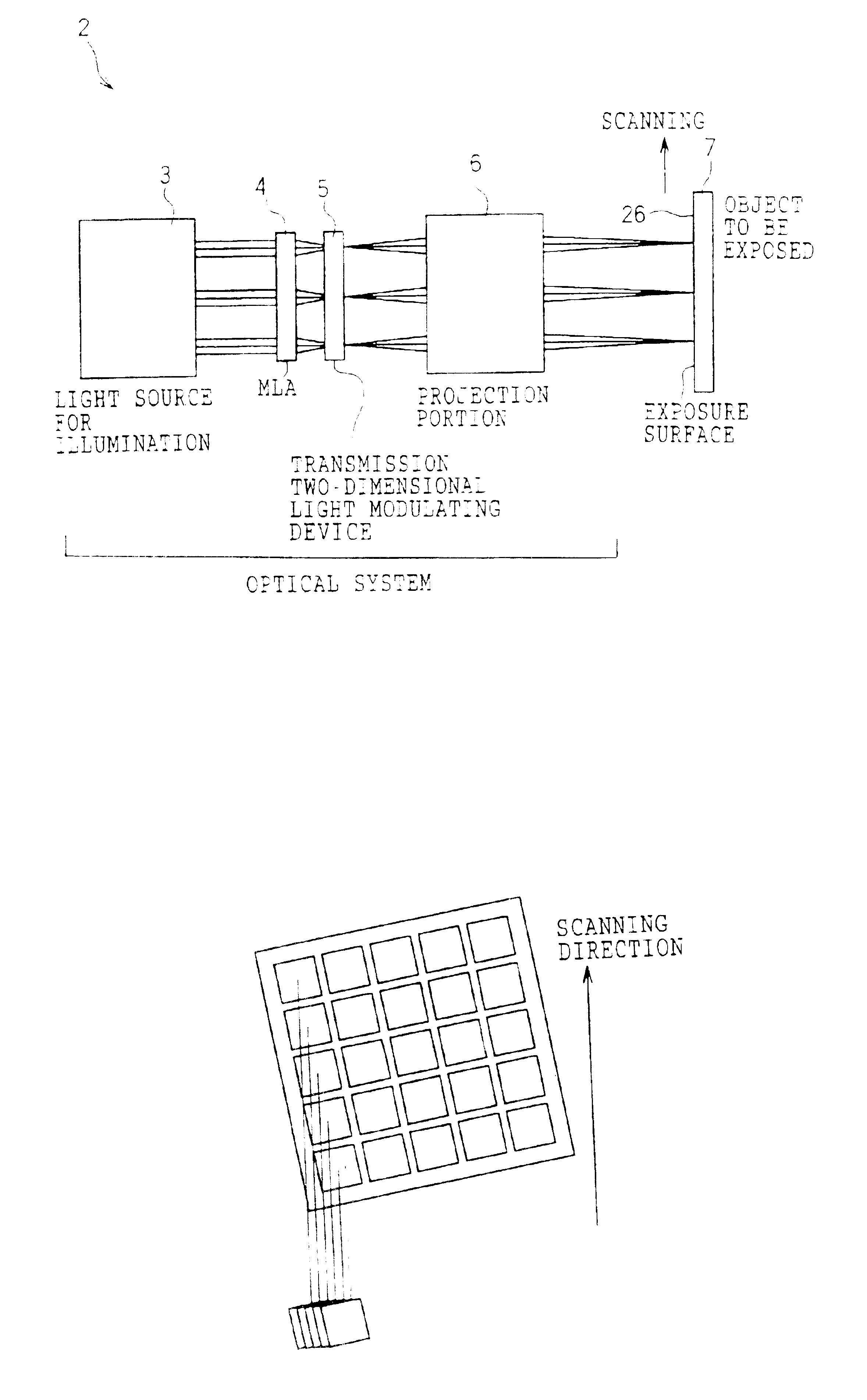
[0046]Initially a first embodiment will be described. FIG. 1 shows the whole of exposure apparatus of the first embodiment. In an exposure apparatus 2 of the first embodiment, a plane-shaped light beam emitted from a light source for illumination 3 is incident to a microlens array (hereinafter referred to as MLA) 4, and a transmission two-dimensional light modulating device 5 is irradiated with the light beam condensed with MLA 4. Each microlens in MLA corresponds to each light modulating element in the two-dimensional light modulating device 5, and the microlens is designed and adjusted so that an optical axis and a focal point of the microlens are in alignment with the center of the light modulating element of the light modulating element. The microlens array 4 corresponds to the lens array described in the mode of the invention. A light modulating element is provided corresponding to a pixel of an image to be recorded.

[0047]The incident light from the light sour...

second embodiment

[Second Embodiment]

[0057]A second embodiment will be described below. In the second embodiment, the same components as those of the first embodiment are indicated by the same reference numerals and the description is omitted. As shown in FIG. 3, an exposure apparatus 10 described in the second embodiment includes a light modulating portion 23 in which MLA and the light modulating element are integrated.

[0058]Therefore, it is not necessary to adjust the positioning of MLA and the two-dimensional light modulating device, and cost reduction can be achieved because tolerances of the optical accuracy of MLA and the dimensional accuracy of the pattern of the two-dimensional light modulating device are increased. Since the relative positional accuracy between MLA and the two-dimensional light modulating device is improved, the incident light can be efficiently condensed into the light modulating element and the usability of the light can be also improved. Further, since the relative positi...

third embodiment

[Third Embodiment]

[0085]A third embodiment will be described below. FIG. 15 is a block diagram showing the whole exposure apparatus of a third embodiment, FIG. 16 is a sectional view of a transmission two-dimensional light modulating device built in the exposure apparatus of the third embodiment, FIG. 17 is a partially expanded sectional side view of the transmission two-dimensional light modulating device shown in FIG. 16, and FIG. 18 is a partially expanded plan view of FIG. 17. In the third embodiment, the same components as those of the second embodiment are indicated by the same reference numerals and the description is omitted.

[0086]As shown in FIG. 15, a transmission two-dimensional light modulating device 201 is built in an exposure apparatus 200 described in the third embodiment. The transmission two-dimensional light modulating device 201 includes the two-dimensional light modulating device 203 in which micro electro-mechanical light modulating elements are two-dimensional...


PUM

PropertyMeasurementUnit
diameteraaaaaaaaaa
refractive indexaaaaaaaaaa
transmittanceaaaaaaaaaa

Abstract

A light modulating device comprising a plurality of light modulating elements modulating the light that is incident thereto and emitting the light, wherein each of the light modulating elements is formed from a micro electronic machinery which is two-dimensionally arranged, and the transmittance can be controlled so as to vary for each of the light modulating elements. The light modulating device further comprises a lens array on a light-incident side of the light modulating elements, and the lens array condenses the incident light, which impinges on each of the light modulating elements, into a region whose area is smaller than an area occupied by each of the light modulating elements at a light-incident side thereof. Consequently, the light modulating device, in which usability of the light is improved and resolution is increased in the projection exposure, and the exposure apparatus using the same can be obtained.

Description

CROSS-REFERENCE TO RELATED APPLICATION[0001]This application claims priority under 35USC 119 from Japanese Patent Applications No. 2002-167402 and No. 2003-129108, the disclosure of which is incorporated by reference herein.BACKGROUND OF THE INVENTION[0002]1. Field of the Invention[0003]The present invention relates to a light modulating device in which a plane-shaped light beam is incident and its transmittance is changed to perform exposure and an exposure apparatus using the same, more specifically relates to the optimum device for a system performing on-demand direct photolithography, particularly it is preferable for the system, which applies projection exposure by using the two-dimensional light modulating device, such as an image forming apparatus and a projector.[0004]2. Description of the Related Art[0005]In recent years, the exposure apparatus for performing the on-demand direct photolithography of a pattern image onto a photosensitive material without using a photomask is...

Claims


Application Information

Patent Timeline
Patent Type & Authority Patents(United States)
IPC IPC(8): G03F7/20H04N5/74B81B3/00B81B7/04G02B26/02G02B3/00G02B5/00G03F7/207H01L21/027
CPCG03F7/70275G03F7/70291G03F7/70391H04N5/7416
Inventor KIMURA, KOICHISUNAGAWA, HIROSHI
Owner FUJIFILM HLDG CORP
Why Eureka
Try Eureka