Method for fabricating a semiconductor device by transferring a layer to a support with curvature

a technology of curvature and semiconductor devices, applied in non-linear optics, instruments, optics, etc., can solve the problems of narrow space inside the vehicle and complex installation work

Inactive Publication Date: 2005-10-11
SEMICON ENERGY LAB CO LTD
View PDF14 Cites 130 Cited by
  • Summary
  • Abstract
  • Description
  • Claims
  • Application Information

AI Technical Summary

Benefits of technology

[0023]Furthermore, as another peeling method, a peeling method may be used in which a membrane stress between two layers is utilized for peeling. This peeling method can cleanly, easily separate in an oxide layer or in the interface by a physical unit with no film removal (peeling) even through such processes, in which a metal layer, preferably a metal nitride layer is deposited on a substrate, an oxide layer is further deposited on the metal nitride layer, devices are formed over the oxide layer, and then the deposition process or annealing at temperatures of 500° C. or above is performed. For further facilitating the peeling, annealing or laser light irradiation may be performed before peeling by the physical unit.
[0026]Moreover, along the inner walls, doors and seats of the vehicles, or along car dashboards, the display device having the organic light emitting diode with the curvature matched with the curved surfaces is bonded with no curve as it is, whereby images and meters can be displayed. It is fine only to bond the display device fabricated according to the invention along the curved surface, and thus the installation work is significantly simple, not requiring partial work to the inner walls, doors, seats and dashboards in particular. Besides, in the automobiles, for example, when the car is right-handled, a dead angle exists left backside because a part of a car body (a portion between window glasses) is there. However, when the display device fabricated according to the invention is installed in the portion between the window glasses, and a camera capable of shooting in the dead angle direction is mounted outside the car to connect them each other, a driver can confirm the dead angle. Particularly, the display device having the organic light emitting diode is the display device that is superior in moving pictures to the liquid crystal display device and has a wider viewing angle.
[0028]In the vehicles, when the curvature radius of the curved surface in the installed display device ranges from 50 to 200 cm, the TFT and the organic light emitting diode can be driven without problems.

Problems solved by technology

Traditionally, the displays have had flat surfaces, causing spaces inside the vehicles to narrow or the installation work to be complex that a wall is cut out to fit and install a flat display.

Method used


Image

  • Method for fabricating a semiconductor device by transferring a layer to a support with curvature
  • Method for fabricating a semiconductor device by transferring a layer to a support with curvature
  • Method for fabricating a semiconductor device by transferring a layer to a support with curvature

Examples


embodiment

[Embodiment 1]

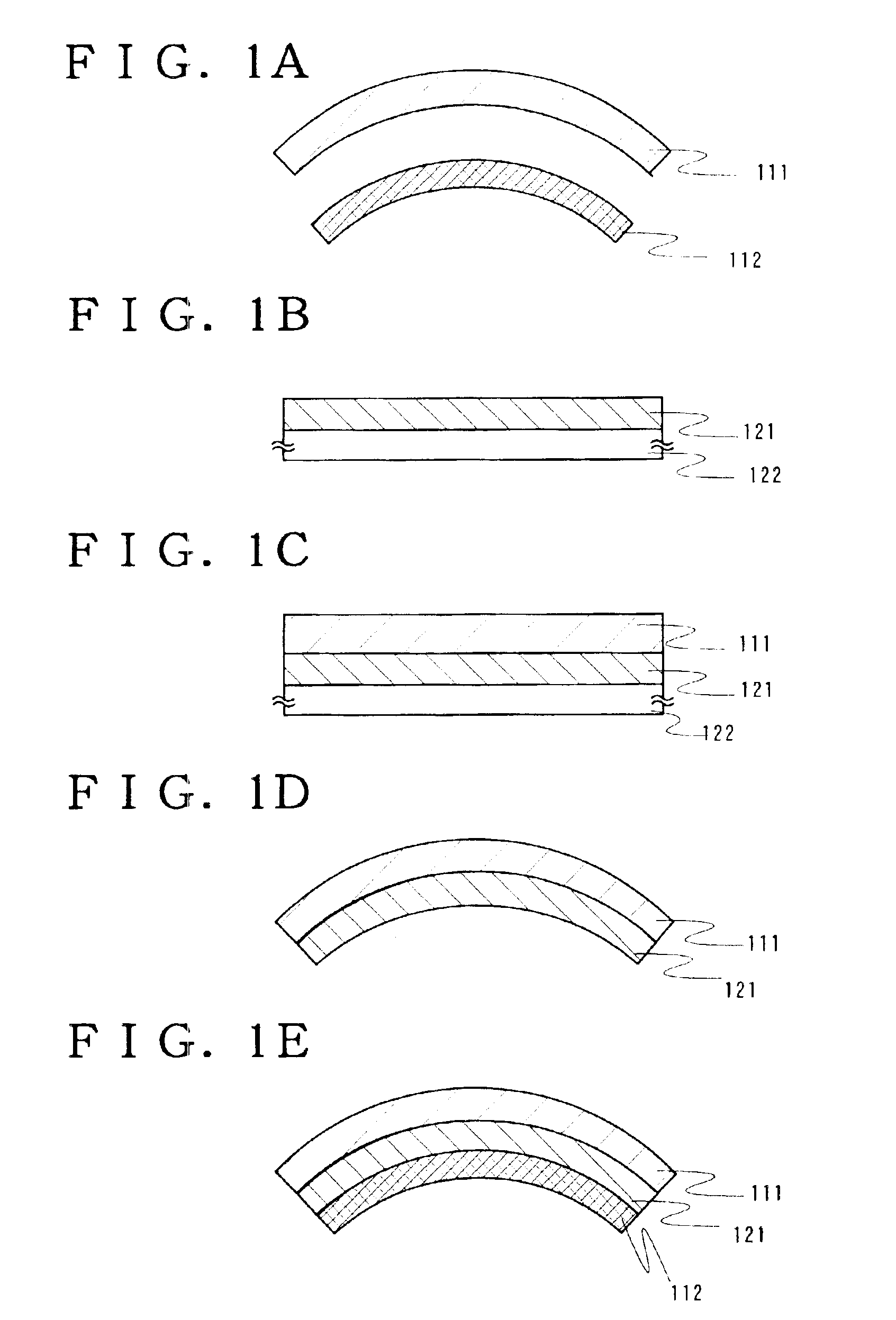
[0052]In the embodiment, the procedures to fabricate a light emitting device having an organic light emitting diode (OLED) are shown in FIGS. 3A to 3E.

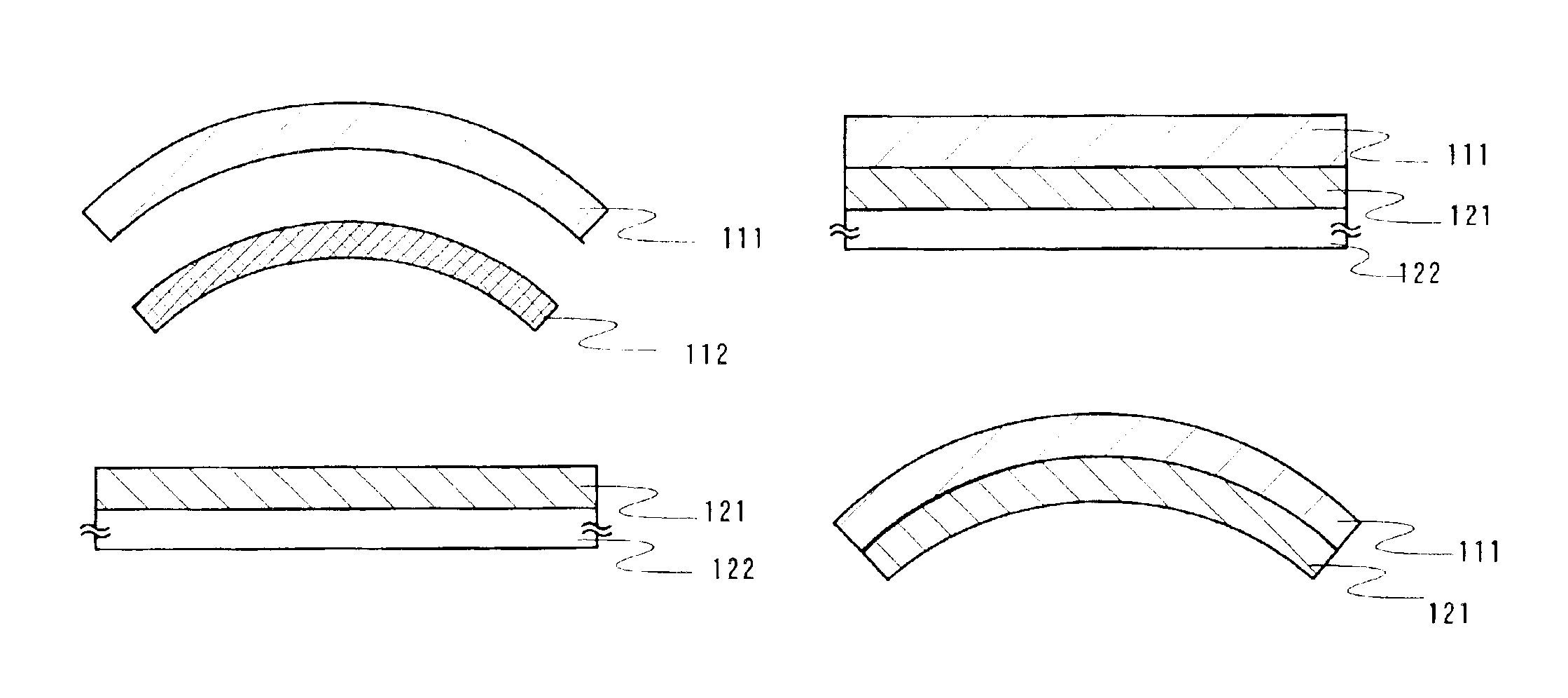
[0053]As shown in FIG. 3A, a first material layer 312 is formed over a substrate 311. As the first material layer 312, it may have compressive stress or may have tensile stress immediately after the deposition. It is important to use materials that do not generate abnormality in peeling due to annealing in forming the peeled layer and the irradiation of laser light and have tensile stress in the range of 1 to 1×10¹⁰ (Dyne / cm2) after the peeled layer is formed. Typically, nitrides or metals are preferable. A representative example is a single layer formed of an element selected from W, WN, TiN and TiW, an alloy material or compound material having a principal component of the elements, or a laminated layer of these. In addition, it is fine to use sputtering for the first material layer 312.

[0054]For the substrate 311, gla...

embodiment 2

[Embodiment 2]

[0073]In the embodiment, the procedures to fabricate a liquid crystal display device are shown in FIGS. 4A to 4E.

[0074]As shown in FIG. 4A, a first material layer 412 is deposited over the substrate 411. As the first material layer 412, it may have the compressive stress or may have tensile stress immediately after film deposition. However, it is important to use materials that do not generate abnormality in peeling due to annealing in forming the peeled layer and the irradiation of laser light and have the tensile stress in the range of 1 to 1×10¹⁰ (Dyne / cm2) after the peeled layer is formed. Typically, nitrides or metals are preferable. A representative example is a single layer formed of an element elected from W, WN, TiN and TiW, an alloy material or a compound material having a principal component of these elements, or a laminated layer of these. In addition, it is fine to use sputtering for the first material layer 412.

[0075]As the substrate 411, glass, silica an...

embodiment 3

[Embodiment 3]

[0091]In the embodiment, FIG. 5 shows an apparatus for fabricating a light emitting device having an organic light emitting diode. In addition, the apparatus shown in the embodiment allows fabricating the light emitting device shown in the embodiment 1.

[0092]FIG. 5 shows an apparatus for depositing a light emitting layer (EL layer) of the organic light emitting diode by the dry deposition method of low weight molecular organic compounds. The apparatus is mainly configured of transport chambers for transferring substrates, delivery chambers for delivery, deposition chambers for depositing various thin films, and an encapsulation chamber for encapsulation. Each chamber is equipped with an exhaust system for achieving necessary vacuum degrees or a system for generating a gas atmosphere such as N2. In addition, the separate chambers are connected by gate valves. The substrates are transferred by transfer robots.

[0093]First, a substrate 501c necessary to fabricate an organi...


PUM

PropertyMeasurementUnit
curvature radiiaaaaaaaaaa
temperaturesaaaaaaaaaa

Abstract

The object of the invention is to provide a method for fabricating a semiconductor device having a peeled layer bonded to a base material with curvature. Particularly, the object is to provide a method for fabricating a display with curvature, more specifically, a light emitting device having an OLED bonded to a base material with curvature. An external force is applied to a support originally having curvature and elasticity, and the support is bonded to a peeled layer formed over a substrate. Then, when the substrate is peeled, the support returns into the original shape by the restoring force, and the peeled layer as well is curved along the shape of the support. Finally, a transfer object originally having curvature is bonded to the peeled layer, and then a device with a desired curvature is completed.

Description

BACKGROUND OF THE INVENTION[0001]The present invention relates to a method for fabricating a semiconductor device having a circuit configured of a thin film transistor (hereafter, it is called a TFT) in which a peeled layer that has been peeled is bonded and transferred to a base material, particularly to a method for transferring a circuit configured of a TFT to a support with curvature.[0002]In recent years, a technique has been receiving attention in which a semiconductor thin film (a thickness of about a few to a few hundreds nanometers) formed over a substrate having an insulated surface is used to configure TFTs. The TFT is widely used for electronic devices such as ICs and electro-optic devices, which has been urged to develop as a switching device for image display devices.[0003]In addition, an attempt has been made to install various display devices on vehicles such as automobiles and aircrafts, including display devices for navigation systems, operation screen display devi...

Claims


Application Information

Patent Timeline
Patent Type & Authority Patents(United States)
IPC IPC(8): H01L21/70H01L21/762H01L21/20H01L21/02H01L21/00H01L51/56H01L51/40H01L51/50H01L51/05H01L51/00H05B44/00
CPCG02F1/133305H01L21/2007H01L21/67092H01L21/6835H01L21/76251H01L27/1214H01L27/1266H01L29/66757H01L29/78603H01L51/0097H01L27/156H01L27/1259H01L27/3244H01L51/0024H01L51/003H01L51/56H01L2221/6835H01L2221/68363H01L2227/326H01L2924/30105H01L2924/3025Y02E10/549H01L27/1218H01L27/124H01L27/1262H10K59/12H10K71/50H10K71/80H10K77/111H10K59/1201H10K71/00H10K2102/311H10K59/123H10K59/131H10K59/1213G02F1/1368G02F1/1339G02F1/13394G02F1/1341
Inventor YAMAZAKI, SHUNPEIMURAKAMI, MASAKAZUTAKAYAMA, TORUMARUYAMA, JUNYA
Owner SEMICON ENERGY LAB CO LTD
Why Eureka
Try Eureka