Method for fabricating electrical connecting element

a technology of electrical connecting elements and electrical components, which is applied in the direction of printed circuit parts, electrical apparatus, printed circuit non-printed electric components association, etc., can solve the problems of piercing spots and protrusions, and achieve the effect of more reliable and efficien

Inactive Publication Date: 2005-10-18
DYCONEX PATENTE
View PDF6 Cites 10 Cited by
  • Summary
  • Abstract
  • Description
  • Claims
  • Application Information

AI Technical Summary

Benefits of technology

[0008]It is therefore an object of the invention to provide a method for the fabrication of microvias that overcomes drawbacks of existing me...

Problems solved by technology

If, however, the substrate layer at the pierced spot is free ...

Method used


Image

  • Method for fabricating electrical connecting element
  • Method for fabricating electrical connecting element
  • Method for fabricating electrical connecting element

Examples


Embodiment Construction

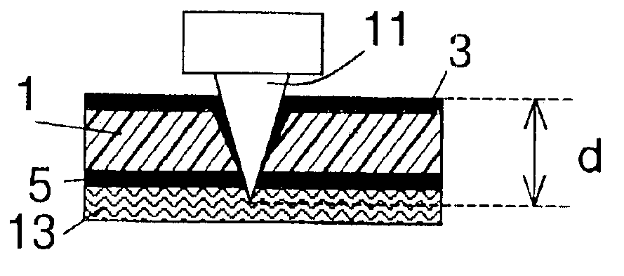
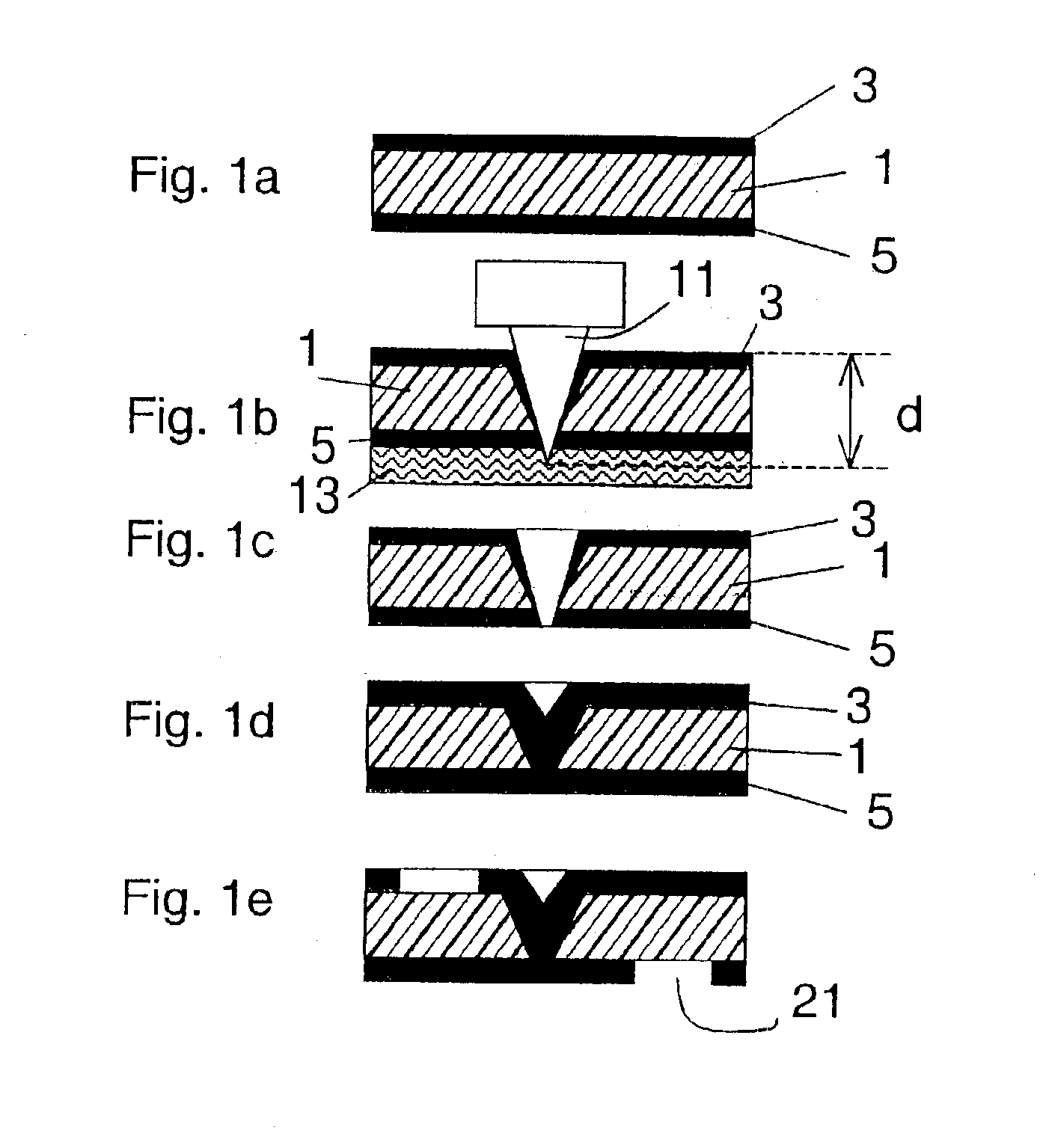
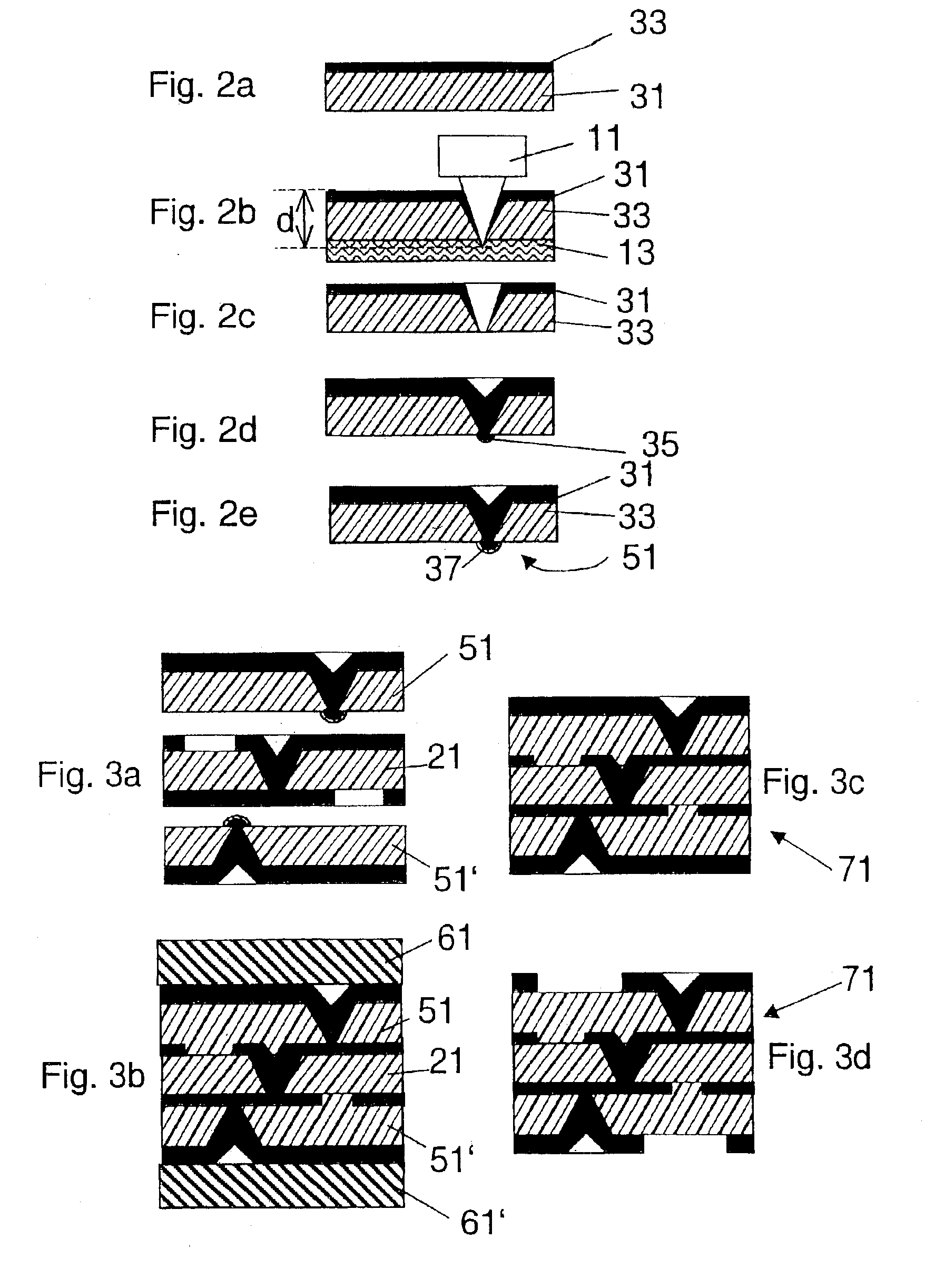
[0017]FIGS. 1a through 1e show a process to manufacture PCB / HDI substrates or semi-finished products for the production thereof by means of a micro-perforation technique. In the following, with reference to FIGS. 1a-1e, 2a-2e and 3a-3d a process for manufacturing a four-layer build-up is described. It should be noted, however, that the described process can also be used to produce an electrical connecting element of 2 layers, 3 layers, 5 layers, 6 layers or any other number of layers. A PCB / HDI substrate of two layers, for example, can be produced using the procedure of FIGS. 1a-1e. Also, a product produced according to FIGS. 2a-2e may by itself serve as a two layer PCB / HDI substrate. In order to produce a PCB / HDI substrate of more layers, to such a substrate produced in accordance with FIGS. 1a-1e (as a semi-finished product), the appropriate number of semi-finished products produced according to FIGS. 2a-2e has to be added.

[0018]In FIG. 1a, the core base material 1, which is alrea...


PUM

PropertyMeasurementUnit
Thicknessaaaaaaaaaa
Electrical conductoraaaaaaaaaa
Distanceaaaaaaaaaa

Abstract

A method for manufacturing electrical connecting elements or semifinished products. Microvias are formed in a dielectric substrate layer by piercing a substrate layer (1) through a first conducting layer (3), which essentially covers an entire side of the substrate. The perforation depth (d) is at least equal to the total thickness of the substrate and the first conducting layer. The conductor material of the first conducting layer (3), during the piercing step, is deformed so that it partially covers the wall of the hole fabricated by the piercing process. Plating the first conducting layer with additional conductor material bridges the little remaining distance between the conductor material and the opposite side of the substrate layer.

Description

BACKGROUND OF THE INVENTION[0001]1. Field of the Invention[0002]The present invention relates to methods for fabricating electrical connecting elements such as Printed Circuit Boards (PCBs), High-Density-Interconnects (HDIs), Ball-Grid-Array (BGA) substrates, Chip Scale Packages (CSP), Multi-Chip-Module-(MCM) substrates, etc. The present invention also relates to an electrical connecting element and to an apparatus for fabricating electrical connecting elements.[0003]2. Description of Related Art[0004]In modern circuit board technology, due to increasing miniaturization, conventionally drilled through holes are increasingly being replaced by microvias. Methods for fabricating such microvias include laser drilling and plasma drilling as well as photochemical structuring. A new method for fabricating microvias has been disclosed in WO 00 / 13062. This new technology approach, the Micro-Perforation, is a method including mechanical embossing of micro-holes into deformable dielectric mate...

Claims


Application Information

Patent Timeline
IPC IPC(8): H01L23/48H01L23/498H05K3/02H05K3/04H05K3/40H05K3/00H05K3/46H05K3/34H05K1/18H05K1/14H05K1/16H05K1/11H05K3/36H05K1/02
CPCH01L23/49827H05K3/4614H05K3/4652H05K3/4084Y10T29/49167H05K2201/0379H05K2201/09481H05K2201/09509H05K2201/09827H05K2203/0195H05K2203/1189H01L2924/0002Y10T29/49155Y10T29/49165Y10T29/49126H01L2924/00
Inventor SCHMIDT, WALTER
Owner DYCONEX PATENTE
Why Eureka
Try Eureka