
Integrated circuit with multiple microcode ROMs

Inactive Publication Date: 2005-10-18
GLOBALFOUNDRIES INC
View PDF11 Cites 9 Cited by
  • Summary
  • Abstract
  • Description
  • Claims
  • Application Information

AI Technical Summary

Benefits of technology

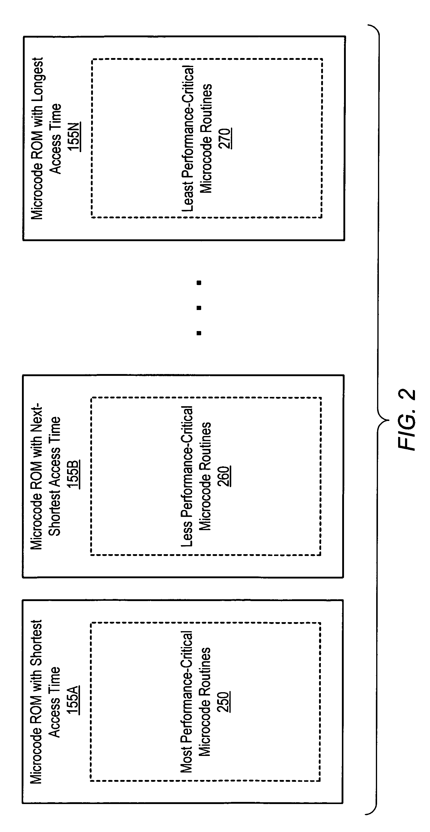
[0016]In some embodiments in which the access times of the microcode ROMs differ, fewer than all of the microcode routines may be stored in one of the microcode ROMs with the smallest access time. For example, in an integrated circuit with two microcode ROMs one of the microcode ROMs may have an access time of one clock cycle and the other microcode ROM may have an access time of two or more clock cycles. The microcode ROM with the access time of one clock cycle may not have a large enough capacity to store all of the microcode routines.
[0017]Microcode routines that are executed relatively infrequently and/or that tend to be executed at times in which microcode ROM performance does not control processor efficiency may be referred to as less performance-critical than microcode routines

Problems solved by technology

Certain instructions within the x86 instruction set are quite complex, specifying multiple operations to be performed.
While it may be possible to implement hardware to execute any instruction directly, the cost of such implementation in terms of the number of transistors required and / or die area needed may be prohibitive in some cases.
In the case of an instruction set like the x86 instruction set mentioned above, which is rich in complex instructions, the hardware required to execute all instructions directly may be enormous.
In fact, current integrated circuit production methods may not be adequate to produce a single chip capable of executing all x86 instruction directly in hardware.
This may become problematic when attempting to implement a integrated circuit capable of executing an instruction set rich in complex instructions (like the x86 instruction set) and at the same time having the highest possible clock speed, as described in more detail below.
This propagation delay may be significant in the design of an integrated circuit's microcode ROM.
For a microcode ROM that occupies a large area on the processor die, signal propagation delay as described above can result in a significantly greater delay in outputting data from a line whose memory elements are located far from the decode logic.
A microcode ROM with enough capacity to store all the microcode routines of a complex instruction set may occupy such a large area on the processor die that it is incapable of the desired access time.
If a microcode ROM cannot output operations at a rate that is greater than or equal to the rate at which the operations can be executed, the processor will operate at less than maximum efficiency.
One microcode ROM may consume a different amount of power (on average during operation) than one of the other microcode ROMs.
The microcode ROM with the access time of one clock cycle may not have a large enough capacity to store all of the microcode routines.

Method used


Image

  • Integrated circuit with multiple microcode ROMs
  • Integrated circuit with multiple microcode ROMs
  • Integrated circuit with multiple microcode ROMs

Examples


Embodiment Construction

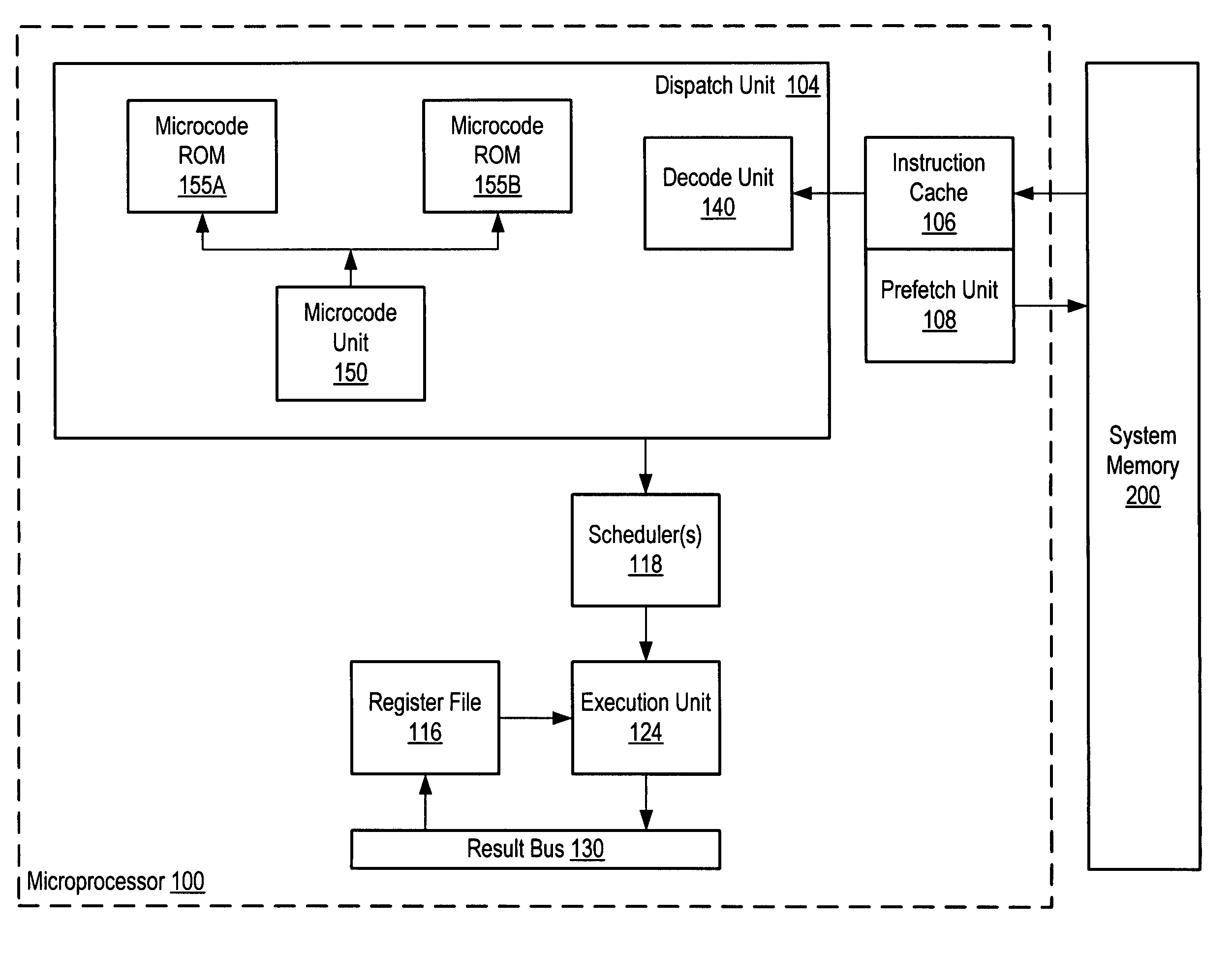
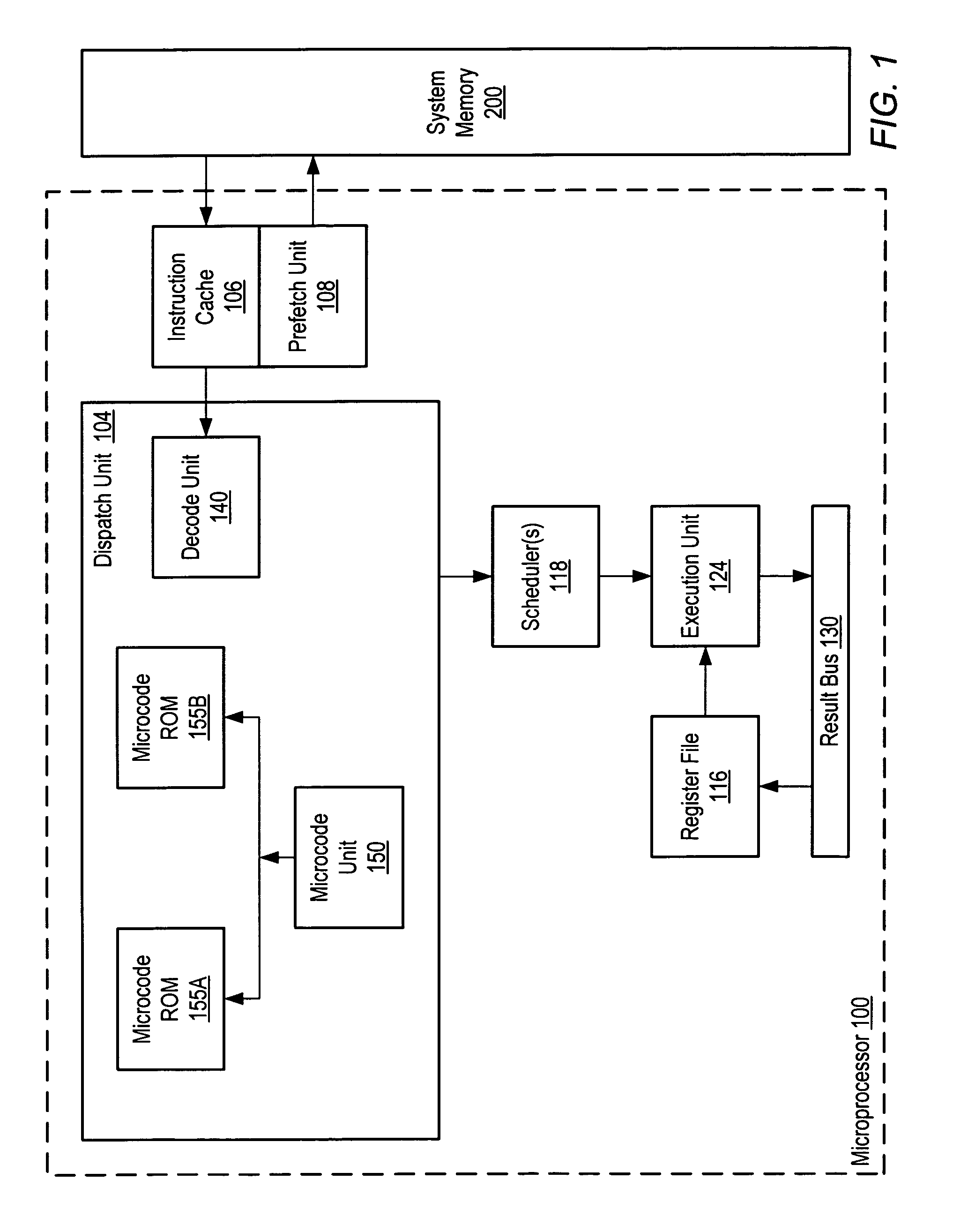
[0026]FIG. 1 is a block diagram of logical components included in a microprocessor 100, according to one embodiment. Microprocessor 100 may be implemented as a single integrated circuit. Microprocessor 100 may include a microcode unit 150 and multiple independently accessible microcode ROMs 155. Microprocessor 100 is configured to execute instructions stored in a system memory 200. In some embodiments, the microprocessor 100 may be designed to be compatible with the x86 architecture. Note that microprocessor 100 may also include and / or be coupled to many other components in addition to those shown here. Additionally, the interconnections between logical components may vary between embodiments.

[0027]Microprocessor 100 may include an instruction cache 106. Microprocessor 100 may include a prefetch unit 108 coupled to the system memory 200. Prefetch unit 108 may prefetch instruction code from the system memory 200 for storage within instruction cache 106. In one embodiment, prefetch un...


PUM


Abstract

Integrated circuits having multiple independently accessible microcode ROMs. An integrated circuit may include a microcode unit and a plurality of microcode ROMs fabricated within the same integrated circuit. The microcode unit may be configured to receive a microcoded instruction and to identify a microcode routine that corresponds to the microcoded instruction. The microcode ROMs may collectively store the microcode routines that implement the microcoded instructions of a complex instruction set, and different microcode ROMs may have different access times. At least one of the microcode ROMs may output operations included in the microcode routine in response to the microcode unit identifying the microcode routine. Microcode routines having more performance criticality may be stored in a microcode ROM having a smaller access latency than the access latency of a microcode ROM in which microcode routines having less performance criticality are stored.

Description

BACKGROUND OF THE INVENTION[0001]1. Field of the Invention[0002]This invention is related to the field of integrated circuits, and more particularly, to storing and processing microcoded instructions within an integrated circuit.[0003]2. Description of the Related Art[0004]Instructions processed in an integrated circuit are encoded as a sequence of ones and zeros. For some processor architectures, instructions may be encoded with a fixed length, such as a certain number of bytes. For other architectures, such as the x86 architecture, the length of instructions may vary. The x86 integrated circuit architecture specifies a variable length instruction set (i.e., an instruction set in which various instructions are each specified by differing numbers of bytes). For example, the 80386 and later versions of x86 integrated circuits employ between 1 and 15 bytes to specify a particular instruction. Instructions have an opcode, which may be 1–2 bytes, and additional bytes may be added to spe...

Claims


Application Information

Patent Timeline
IPC IPC(8): G06F9/22
CPCG06F9/3017G06F9/30181G06F9/26G06F9/30145
Inventor MCMINN, BRIAN D.PICKETT, JAMES K.
Owner GLOBALFOUNDRIES INC
Learn More