Method for making contactless cards

a contactless card and card body technology, applied in the direction of instruments, semiconductor/solid-state device details, dynamo-electric converter control, etc., can solve the problems of mechanical strength and tensile fragility of the connection, the protrusion suffers damage affecting the quality of the electrical connection, and the card thickness is reduced, so as to facilitate the penetration of the protrusions and soften the antenna material

Inactive Publication Date: 2005-10-25
GEMPLU
View PDF9 Cites 59 Cited by
  • Summary
  • Abstract
  • Description
  • Claims
  • Application Information

AI Technical Summary

Benefits of technology

[0017]According to yet another embodiment, the antenna is produced from a thermoplastic material loaded with metallic particles, the chip is glued in advance to an insulating sheet to the format of the smart card to be produced, and then the connection of the chip to the antenna is effected by hot lamination. In this case also, the heat softens the antenna material whilst the lamination facilitates the penetration of the protrusions into the softened material.

Problems solved by technology

One of the main problems which it is necessary to resolve in the manufacture of such cards is the connection of the antenna to the integrated-circuit chip which provides the electronic functioning of the card.
Another problem which it is necessary to resolve is the reduction of the thickness of the card as far as possible.
However, the interconnection unit thus obtained has problems of mechanical strength and tensile fragility of the connection.
This is because, when the chip is subjected to mechanical stresses, the protrusions suffer damage affecting the quality of the electrical connection.
The mechanical stresses can even go as far as causing the rupture of the protrusions and consequently the pulling away of the chip.
The contactless smart cards produced according to this prior method therefore have a relatively short service life.
In this case, however, a significant excess thickness appears because of the presence of the glue and the protrusions.
In addition, the manufacture of the card requires an additional step of dispensing the dots of glue.

Method used


Image

  • Method for making contactless cards
  • Method for making contactless cards

Examples


Embodiment Construction

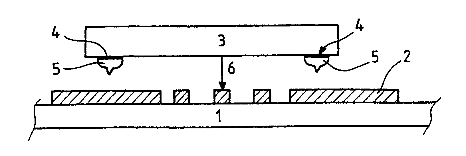
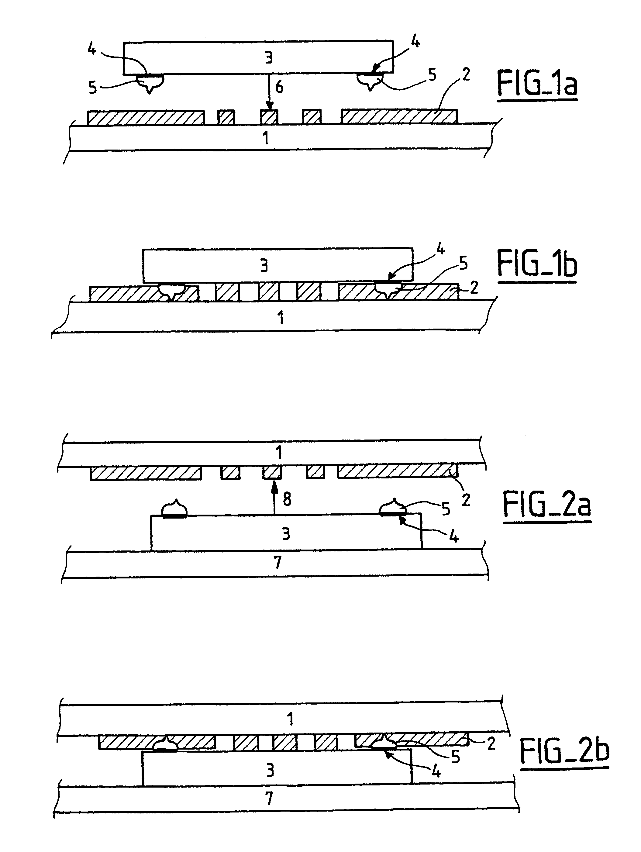
[0021]FIGS. 1a and 1b depict a chip 3 during its mounting on an antenna 2. The interconnection assembly formed by the chip 3 and antenna 2 is intended to be inserted in a contactless smart card of ultrafine thickness less than the standard ISO thickness.

[0022]A preliminary step of the manufacturing method according to the invention consists of forming metallised protrusions 5 on contact pads 4 on the chip 3. The protrusions 5 are intended to provide the electrical connection between the chip 3 and antenna 2. They are consequently necessarily produced from a conductive material. They may for example be produced from gold, or from a polymer material loaded with metallic particles.

[0023]Preferably the protrusions 5 are produced on two contact pads 4 on the chip in order to be able to produce a connection on conductive areas of the antenna 2 situated at its ends.

[0024]Given that the protrusions 5 are intended to be embedded in the thickness of the antenna 2, they preferably have a thick...


PUM

PropertyMeasurementUnit
thicknessaaaaaaaaaa
thicknessesaaaaaaaaaa
thicknessaaaaaaaaaa

Abstract

A method for producing contact-free chip card includes embedding metallized bumps of the chip into an antenna as the chip is mounted on the antenna.

Description

[0001]This disclosure is based upon, and claims priority from French Patent Application No. 98 / 02844, filed Mar. 9, 1998, and International Application No. PCT / FR99 / 00445, filed Feb. 26, 1999, the contents of which are incorporated herein by reference.BACKGROUND OF THE INVENTION[0002]The present invention relates to the manufacture of smart cards, and more particularly cards capable of functioning without contact by means of an antenna integrated into the card.[0003]Such cards are intended for performing various operations such as, for example, banking operations, telephone communications, identification operations, operations of debiting or recharging units of account, and all kinds of operations which can be performed remotely by high-frequency electromagnetic coupling between a transmission / reception terminal and a card placed in the area of action of this terminal.[0004]One of the main problems which it is necessary to resolve in the manufacture of such cards is the connection o...

Claims


Application Information

Patent Timeline
Patent Type & Authority Patents(United States)
IPC IPC(8): G06K19/077G06K19/07B42D15/10
CPCG06K19/07749G06K19/0775Y10T29/49149H01L2224/1134H01L2224/13144H01L2924/01057H01L2924/01079Y10T29/49018Y10T29/49016Y10T29/4913H01L2924/00013H01L2223/6677H01L2224/16238H01L2224/8114H01L2924/00014H01L2224/13099
Inventor PATRICE, PHILIPPE
Owner GEMPLU
Why Eureka
Try Eureka