Methods of forming field effect transistors and field effect transistor circuitry

a field effect transistor and field effect technology, applied in logic circuits using specific components, pulse generators, pulse techniques, etc., can solve problems such as increased sub-threshold current leakage and adversely affecting device performan

Inactive Publication Date: 2005-10-25
MICRON TECH INC
View PDF18 Cites 50 Cited by
  • Summary
  • Abstract
  • Description
  • Claims
  • Application Information

AI Technical Summary

Benefits of technology

[0005]Methods of forming field effect transistors and resultant field effect transistor circuitry are described. In one embodiment, a semiconductive substrate includes a field effect transistor having a body. A first resistive element is received by the substrate and connected between the transistor's gate and the body. A second resistive element is received by the substrate and connected between the body and a refere

Problems solved by technology

While higher drive currents can be achieved by building wider FET devices, tradeoffs are made in valuable wafer real estate.
Larger devices also typically have larger

Method used


Image

  • Methods of forming field effect transistors and field effect transistor circuitry
  • Methods of forming field effect transistors and field effect transistor circuitry
  • Methods of forming field effect transistors and field effect transistor circuitry

Examples


Embodiment Construction

[0024]This disclosure of the invention is submitted in furtherance of the constitutional purposes of the U.S. Patent Laws “to promote the progress of science and useful arts” (Article 1, Section 8).

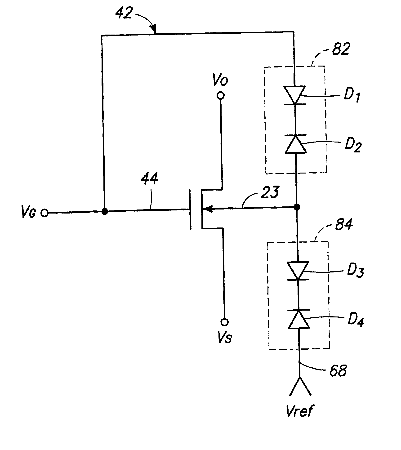
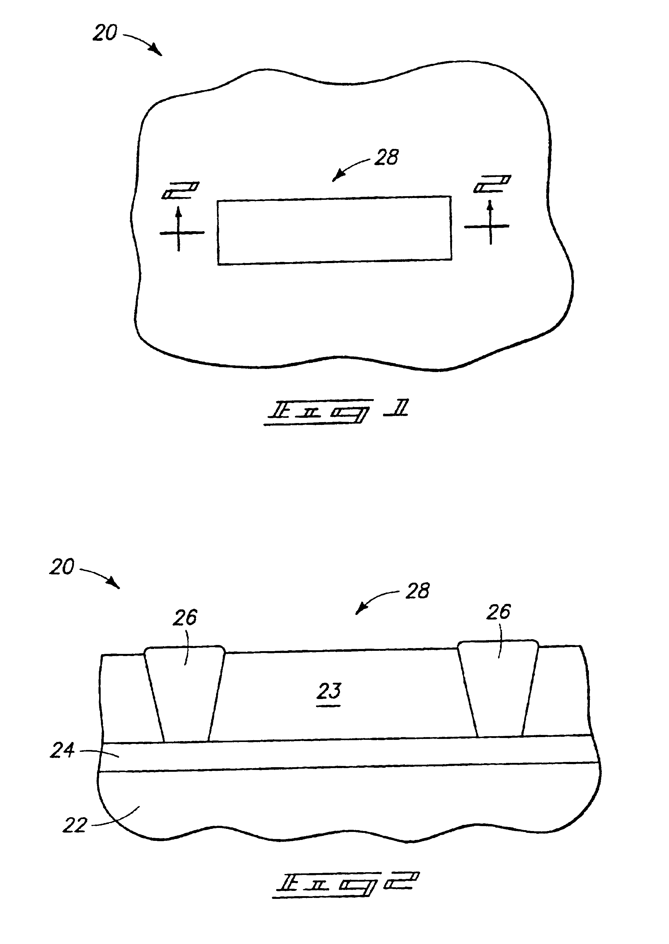
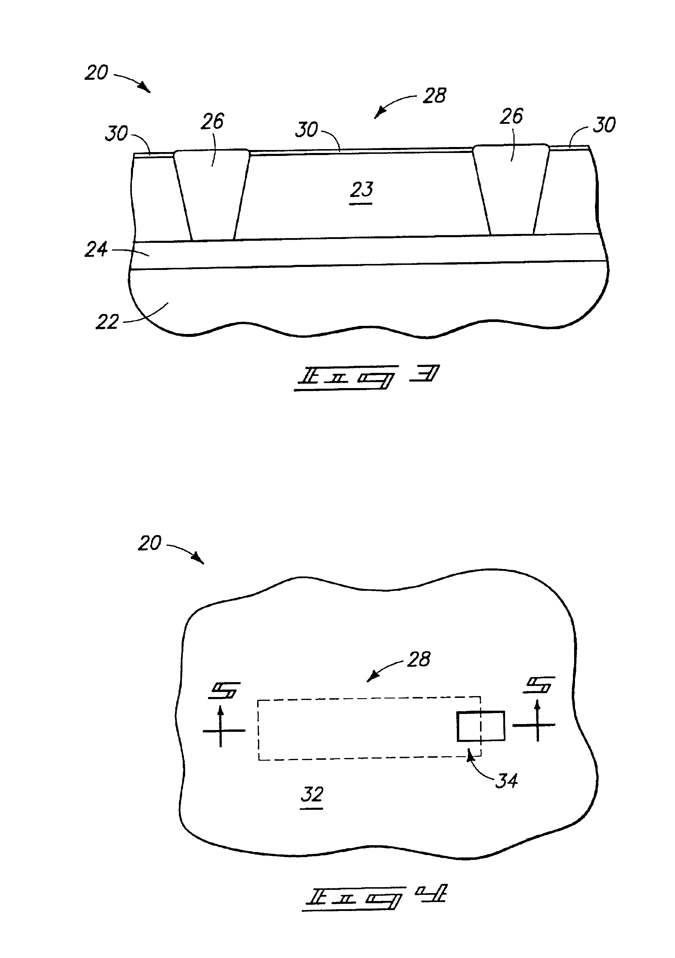
[0025]Referring to FIGS. 1 and 2, a semiconductor wafer fragment 20 includes a semiconductive substrate 22 having a substrate region 23. Region 23 comprises a body of a field effect transistor which is to be formed. In the illustrated example, substrate 22 includes a buried mega eV (MeV) layer 24 and a pair of isolation regions 26 which collectively isolate the body. Where n-channel devices are to be formed, substrate region 23 comprises p-type material and layer 24 comprises n-type material. Where p-channel devices are to be formed, substrate region 23 comprises n-type material and layer 24 comprises p, type material. Layer 24 and isolation regions 26 define an area 28 over or within which field effect transistor circuitry is to be formed. The substrate can comprise any suitable substrat...


PUM


Abstract

Methods of forming field effect transistors and resultant field effect transistor circuitry are described. In one embodiment, a semiconductive substrate includes a field effect transistor having a body. A first resistive element is received by the substrate and connected between the transistor's gate and the body. A second resistive element is received by the substrate and connected between the body and a reference voltage node. The first and second resistive elements form a voltage divider which is configured to selectively change threshold voltages of the field effect transistor with state changes in the gate voltage. In a preferred embodiment, first and second diode assemblies are positioned over the substrate and connected between the gate and body, and the body and a reference voltage node to provide the voltage divider.

Description

CROSS REFERENCE TO ELATED APPLICATION[0001]This patent application is a Continuation Application of U.S. patent application Ser. No. 09 / 545,976, filed Apr. 10, 2000, now U.S. Pat. No. 6,307,238, entitled “Method of Forming Field Effect Transistors and Field Effect Transistor Circuitry”, naming Fernando Gonzalez and Chandra Mouli as inventors, which is a Continuation Application of U.S. patent application Ser. No. 09 / 266,710, filed Mar. 11, 1999, now U.S. Pat. No. 6,121,665, which is a Divisional Application of U.S. patent application Ser. No. 09 / 032,267, filed Feb. 27, 1998, now U.S. Pat. No. 6,271,067, the disclosure of which is incorporated by reference.TECHNICAL FIELD[0002]This invention relates to methods of forming field effect transistors, and to field effect transistor circuitry.BACKGROUND OF THE INVENTION[0003]It is desirable in transistors to be able to drive high currents. Driving high currents can enhance a transistor's operating performance including its operating speed....

Claims


Application Information

Patent Timeline
IPC IPC(8): H01L27/07
CPCH01L27/0727
Inventor GONZALEZ, FERNANDOMOULI, CHANDRA
Owner MICRON TECH INC
Why Eureka
Try Eureka