Method of utilizing dual-layer photoresist to form black matrixes and spacers on a control circuit substrate

a control circuit substrate and photoresist technology, applied in non-linear optics, instruments, optics, etc., can solve the problems of ineffective increase of inability to effectively increase the aperture ratio of the tft-lcd, and inability to achieve long exposure time, etc., to achieve the effect of increasing the process margin and increasing the throughput of products

Inactive Publication Date: 2005-10-25
HANNSTAR DISPLAY CORPORATION
View PDF4 Cites 14 Cited by
  • Summary
  • Abstract
  • Description
  • Claims
  • Application Information

AI Technical Summary

Benefits of technology

[0009]It is another objective of the present invention to provide a method of forming black matrixes and spacers on a control circuit substrate by double layers of photoresist to increase the throughput of products.
[0010]It is still another objective of the present invention to provide a method of forming black matrixes and spacers on a control circuit substrate by dual-layer photoresist to increase the process margin.
[0021]In the foregoing, the invention utilizes the much-improved light transmittance and photosensitivity properties of the transparent photoresist rather than those of the black resin to decrease the thickness needed by black resin used in the prior arts. Hence, the exposure time needed for the black resin used in the prior arts can be greatly reduced to increase greatly the product throughput.

Problems solved by technology

However, the value of the commercial application was not proved until Sharp in Japan developed a liquid crystal display applied in a calculator.
As a result of the limitations of assembling precision, the aperture ratio of the TFT-LCD cannot be effectively increased.
Therefore, a very long exposure time is needed for patterning the black resin to form an ideal pattern, and the throughput of the stepper is seriously affected.

Method used


Image

  • Method of utilizing dual-layer photoresist to form black matrixes and spacers on a control circuit substrate
  • Method of utilizing dual-layer photoresist to form black matrixes and spacers on a control circuit substrate
  • Method of utilizing dual-layer photoresist to form black matrixes and spacers on a control circuit substrate

Examples


embodiment 1

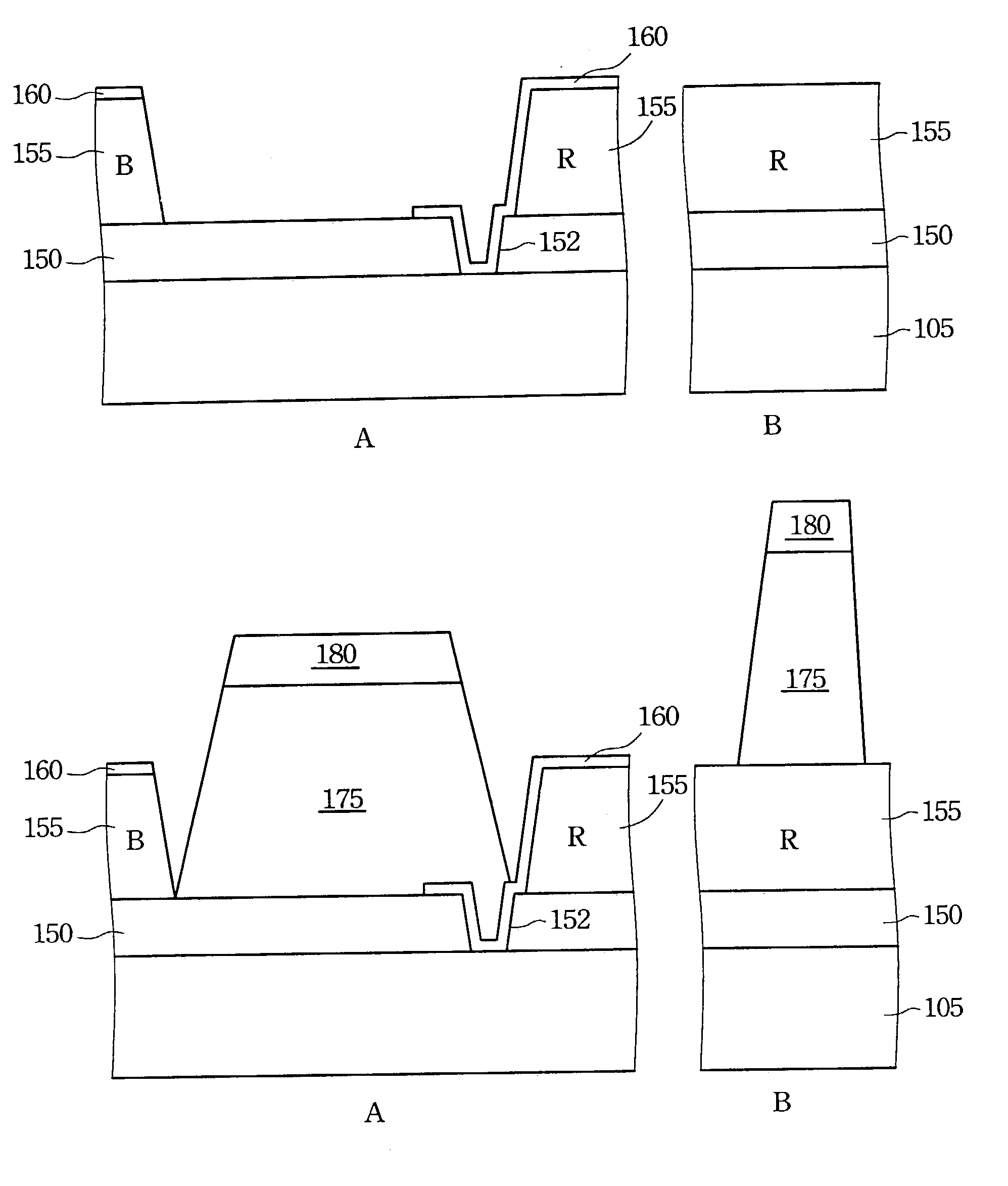
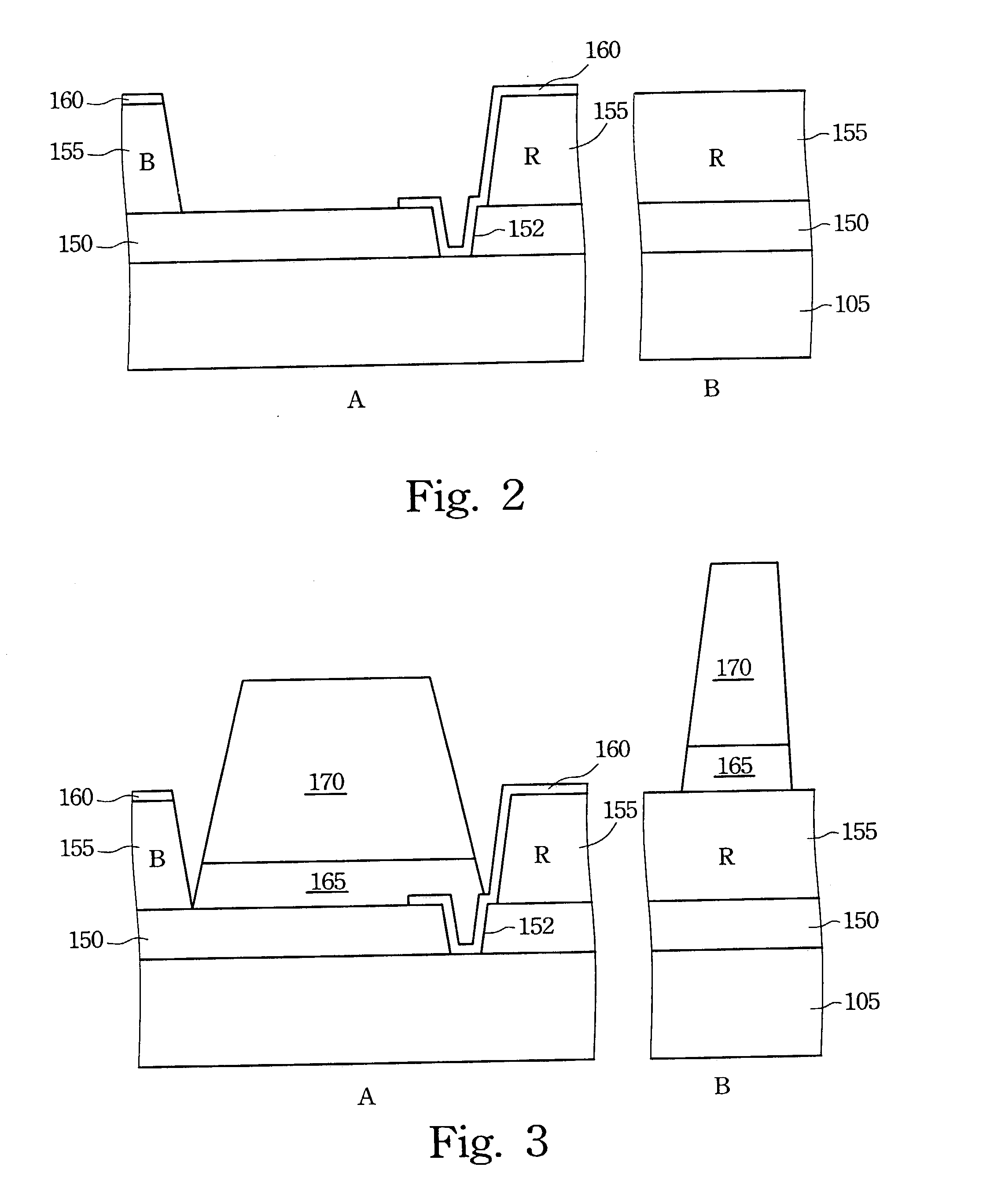
[0031]FIGS. 2 and 3 are cross-sectional diagrams of utilizing dual-layer photoresist to form black matrixes and spacers on a control circuit substrate in FIG. 1 according to a preferred embodiment of this invention. The labels A and B in FIGS. 2 and 3 indicate the cross-sectional views of the cross-sectional lines AA′ and BB′, respectively. The TFT structures are not drawn in the Parts A in FIGS. 2 and 3 to simplify the pictures.

[0032]In FIG. 2, a passivation layer 150 such as a silicon nitride layer is formed by, for example, chemical vapor deposition (CVD) on the control circuit substrate 105 (i.e. the transparent substrate 100 having the control circuit thereon as shown in FIG. 1). The control circuit substrate 105 comprises, for example, a TFT array substrate. Next, the passivation layer 180 is patterned by, for example, photolithography and etching to form contact windows 152 therein to expose drains 130 (not shown in FIG. 2) of the TFT, respectively.

[0033]A color filter layer ...

embodiment 2

[0042]FIGS. 2 and 4 are cross-sectional diagrams of utilizing dual-layer photoresist to form black matrixes and spacers on a control circuit substrate in FIG. 1 according to another preferred embodiment of this invention. The labels A and B in FIGS. 2 and 4 indicate the cross-sectional views of the cross-sectional lines AA′ and BB′, respectively. The TFT structures are not drawn on the Parts A in FIGS. 2 and 4 to simplify the pictures. Besides, a detailed description of FIG. 2 has been given above, and hence is omitted here.

[0043]In FIG. 4, a transparent photoresist is formed on the control circuit 105 having the color filter layer 155 and the pixel electrodes 160 located thereon. Then, the transparent photoresist is soft-baked. A black resin is formed on the black resin and then is soft-baked. Next, the black resin and the transparent photoresist are patterned and hard-baked to form transparent photoresist layers 175 and black resin layers 180. Consequently, black matrixes is forme...


PUM

PropertyMeasurementUnit
optical densityaaaaaaaaaa
thicknessaaaaaaaaaa
thicknessaaaaaaaaaa

Abstract

A method of utilizing dual-layer photoresist to form black matrixes and spacers on a control circuit substrate is provided. The dual-layer photoresist is composed of a layer of black resin and a layer of transparent photoresist. The black resin, of which optical density is greater than three, is mainly used to achieve the effect of black matrix. The transparent photoresist is mainly used to satisfy the needed cell gap between two transparent substrates.

Description

BACKGROUND OF THE INVENTION[0001]1. Field of Invention[0002]The present invention relates to a structure of a color liquid crystal display (LCD) and a method of producing the same. More particularly, the present invention relates to a method of utilizing dual-layer photoresist to form black matrixes and spacers on a control circuit substrate and the LCD structure fabricated by the same method.[0003]2. Description of Related Art[0004]Liquid crystal is a material having properties between those of crystal and liquid. The alignment of the liquid crystal molecules varies with external stimulation such as an electrical field generated by an applied voltage. Hence, this feature of the liquid crystal molecules can be utilized to create a display unit.[0005]Liquid crystal material was discovered in 1888, and applications thereof first appeared in 1963. However, the value of the commercial application was not proved until Sharp in Japan developed a liquid crystal display applied in a calcula...

Claims


Application Information

Patent Timeline
Patent Type & Authority Patents(United States)
IPC IPC(8): G02F1/1362G02F1/1339G02F1/13
CPCG02F1/136209G02F1/13394
Inventor LAN, CHIH-CHIEHHUNG, HUNG-YIWANG, YU-FANG
Owner HANNSTAR DISPLAY CORPORATION
Why Eureka
Try Eureka